- 您现在的位置:买卖IC网 > PDF目录19434 > LMZ14201TZX-ADJ/NOPB (National Semiconductor)IC BUCK SYNC ADJ 1A TO-PMOD-7 PDF资料下载
参数资料
| 型号: | LMZ14201TZX-ADJ/NOPB |
| 厂商: | National Semiconductor |
| 文件页数: | 15/27页 |
| 文件大小: | 0K |
| 描述: | IC BUCK SYNC ADJ 1A TO-PMOD-7 |
| 产品培训模块: | LMZ Power Modules SIMPLE SWITCHER® Regulators SIMPLE SWITCHER Power Modules |
| 视频文件: | Power Design Invitational - Another Geek Moment |
| 标准包装: | 500 |
| 系列: | SIMPLE SWITCHER® |
| 类型: | 非隔离(POL) |
| 输出数: | 1 |
| 电压 - 输入(最小): | 6V |
| 电压 - 输入(最大): | 42V |
| Voltage - Output 1: | 0.8 ~ 6 V |
| 电流 - 输出(最大): | 1A |
| 电源(瓦) - 制造商系列: | 6W |
| 特点: | 带有 UVLO |
| 安装类型: | 表面贴装 |
| 封装/外壳: | TO-PMOD-7,电源模块 |
| 尺寸/尺寸: | 0.40" L x 0.54" W x 0.18" H(10.2mm x 13.8mm x 4.6mm) |
| 包装: | 带卷 (TR) |
| 工作温度: | -40°C ~ 125°C |
| 效率: | 90% |
| 电源(瓦特)- 最大: | 6W |
| 其它名称: | LMZ14201TZX-ADJ |
第1页第2页第3页第4页第5页第6页第7页第8页第9页第10页第11页第12页第13页第14页当前第15页第16页第17页第18页第19页第20页第21页第22页第23页第24页第25页第26页第27页
�� �
�
�LMZ14201�
�www.ti.com�
�SNVS649F� –� JANUARY� 2010� –� REVISED� OCTOBER� 2013�
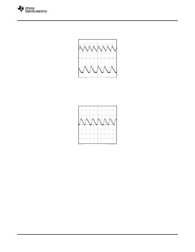
�Following� is� a� comparison� pair� of� waveforms� of� the� showing� both� CCM� (upper)� and� DCM� operating� modes.�
�Figure� 33.� CCM� and� DCM� Operating� Modes�
�V� IN� =� 12V,� V� O� =� 3.3V,� I� O� =� 1� A� /� 0.25� A�
�500 mA/Div�
�2.00� 2� s/Div�
�The� approximate� formula� for� determining� the� DCM/CCM� boundary� is� as� follows:�
�I� DCB� ?� V� O� *(V� IN� –V� O� )/(2*10� μ� H*f� SW(CCM)� *V� IN� )�
�Following� is� a� typical� waveform� showing� the� boundary� condition.�
�Figure� 34.� Transition� Mode� Operation�
�V� IN� =� 24V,� V� O� =� 3.3V,� I� O� =� 0.29� A�
�(16)�
�500 mA/Div�
�2.00� 2� s/Div�
�The� inductor� internal� to� the� module� is� 10� μ� H.� This� value� was� chosen� as� a� good� balance� between� low� and� high�
�input� voltage� applications.� The� main� parameter� affected� by� the� inductor� is� the� amplitude� of� the� inductor� ripple�
�current� (I� LR� ).� I� LR� can� be� calculated� with:�
�I� LR� P-P� =V� O� *(V� IN� -� V� O� )/(10μH*f� SW� *V� IN� )�
�(17)�
�Where� V� IN� is� the� maximum� input� voltage� and� f� SW� is� determined� from� Equation� 10� .�
�If� the� output� current� I� O� is� determined� by� assuming� that� I� O� =� I� L� ,� the� higher� and� lower� peak� of� I� LR� can� be�
�determined.� Be� aware� that� the� lower� peak� of� I� LR� must� be� positive� if� CCM� operation� is� required.�
�POWER� DISSIPATION� AND� BOARD� THERMAL� REQUIREMENTS�
�For� the� design� case� of� V� IN� =� 24V,� V� O� =� 3.3V,� I� O� =� 1A,� T� AMB(MAX)� =� 85°C� ,� and� T� JUNCTION� =� 125°C,� the� device� must�
�see� a� thermal� resistance� from� case� to� ambient� of� less� than:�
�θ� CA� <� (T� J-MAX� —� T� AMB(MAX)� )� /� P� IC-LOSS� -� θ� JC�
�(18)�
�Given� the� typical� thermal� resistance� from� junction� to� case� to� be� 1.9� °C/W.� Use� the� 85°C� power� dissipation� curves�
�in� the� Typical� Performance� Characteristics� section� to� estimate� the� P� IC-LOSS� for� the� application� being� designed.� In�
�this� application� it� is� 0.52W.�
�θ� CA� =� (125� —� 85)� /� 0.52W� —� 1.9� =� 75�
�To� reach� θ� CA� =� 75,� the� PCB� is� required� to� dissipate� heat� effectively.� With� no� airflow� and� no� external� heat,� a� good�
�estimate� of� the� required� board� area� covered� by� 1� oz.� copper� on� both� the� top� and� bottom� metal� layers� is:�
�Board� Area_cm� 2� =� 500°C� x� cm� 2� /W� /� θ� JC�
�(19)�
�Copyright� ?� 2010–2013,� Texas� Instruments� Incorporated�
�Product� Folder� Links:� LMZ14201�
�Submit� Documentation� Feedback�
�15�
�相关PDF资料 |
PDF描述 |
|---|---|
| VE-26T-CY-F2 | CONVERTER MOD DC/DC 6.5V 50W |
| 180-062-113R021 | CONN DB62 MALE HD DIP SLD NICKEL |
| VI-J3D-IZ | CONVERTER MOD DC/DC 85V 25W |
| SWS1005 | PWR SUP 5V 20A SNG OUTPUT |
| VI-J3B-IZ | CONVERTER MOD DC/DC 95V 25W |
相关代理商/技术参数 |
参数描述 |
|---|---|
| LMZ14202 | 制造商:NSC 制造商全称:National Semiconductor 功能描述:2A SIMPLE SWITCHER? Power Module with 42V Maximum Input Voltage |
| LMZ14202_1 | 制造商:NSC 制造商全称:National Semiconductor 功能描述:2A SIMPLE SWITCHER?? Power Module with 42V Maximum Input Voltage |
| LMZ14202_11 | 制造商:NSC 制造商全称:National Semiconductor 功能描述:2A SIMPLE SWITCHER? Power Module with 42V Maximum Input Voltage |
| LMZ14202EVAL/NOPB | 功能描述:电源管理IC开发工具 LMZ14202EVAL BOARD RoHS:否 制造商:Maxim Integrated 产品:Evaluation Kits 类型:Battery Management 工具用于评估:MAX17710GB 输入电压: 输出电压:1.8 V |
| LMZ14202EXT | 制造商:TI 制造商全称:Texas Instruments 功能描述:2A SIMPLE SWITCHER?? Power Module with 42V Maximum Input Voltage for Military and Rugged Applications |
发布紧急采购,3分钟左右您将得到回复。