- 您现在的位置:买卖IC网 > PDF目录19434 > LMZ14201TZX-ADJ/NOPB (National Semiconductor)IC BUCK SYNC ADJ 1A TO-PMOD-7 PDF资料下载
参数资料
| 型号: | LMZ14201TZX-ADJ/NOPB |
| 厂商: | National Semiconductor |
| 文件页数: | 16/27页 |
| 文件大小: | 0K |
| 描述: | IC BUCK SYNC ADJ 1A TO-PMOD-7 |
| 产品培训模块: | LMZ Power Modules SIMPLE SWITCHER® Regulators SIMPLE SWITCHER Power Modules |
| 视频文件: | Power Design Invitational - Another Geek Moment |
| 标准包装: | 500 |
| 系列: | SIMPLE SWITCHER® |
| 类型: | 非隔离(POL) |
| 输出数: | 1 |
| 电压 - 输入(最小): | 6V |
| 电压 - 输入(最大): | 42V |
| Voltage - Output 1: | 0.8 ~ 6 V |
| 电流 - 输出(最大): | 1A |
| 电源(瓦) - 制造商系列: | 6W |
| 特点: | 带有 UVLO |
| 安装类型: | 表面贴装 |
| 封装/外壳: | TO-PMOD-7,电源模块 |
| 尺寸/尺寸: | 0.40" L x 0.54" W x 0.18" H(10.2mm x 13.8mm x 4.6mm) |
| 包装: | 带卷 (TR) |
| 工作温度: | -40°C ~ 125°C |
| 效率: | 90% |
| 电源(瓦特)- 最大: | 6W |
| 其它名称: | LMZ14201TZX-ADJ |
第1页第2页第3页第4页第5页第6页第7页第8页第9页第10页第11页第12页第13页第14页第15页当前第16页第17页第18页第19页第20页第21页第22页第23页第24页第25页第26页第27页
�� �
�
�LMZ14201�
�SNVS649F� –� JANUARY� 2010� –� REVISED� OCTOBER� 2013�
�www.ti.com�
�As� a� result,� approximately� 6� square� cm� of� 1� oz� copper� on� top� and� bottom� layers� is� required� for� the� PCB� design.�
�Additional� area� will� decrease� die� temperature� proportionately.� The� PCB� copper� heat� sink� must� be� connected� to�
�the� exposed� pad.� Approximately� thirty� six,� 8mils� thermal� vias� spaced� 59mils� (1.5� mm)� apart� must� connect� the� top�
�copper� to� the� bottom� copper.� For� an� example� of� a� high� thermal� performance� PCB� layout� of� approximately� 31�
�square� cm� area.� Refer� to� the� Evaluation� Board� application� note� AN-2024� SNVA422� .� For� more� information� on�
�thermal� design� see� AN-2020� SNVA419� and� AN-2026� SNVA424� .�
�PC� BOARD� LAYOUT� GUIDELINES�
�PC� board� layout� is� an� important� part� of� DC-DC� converter� design.� Poor� board� layout� can� disrupt� the� performance�
�of� a� DC-DC� converter� and� surrounding� circuitry� by� contributing� to� EMI,� ground� bounce� and� resistive� voltage� drop�
�in� the� traces.� These� can� send� erroneous� signals� to� the� DC-DC� converter� resulting� in� poor� regulation� or� instability.�
�Good� layout� can� be� implemented� by� following� a� few� simple� design� rules.�
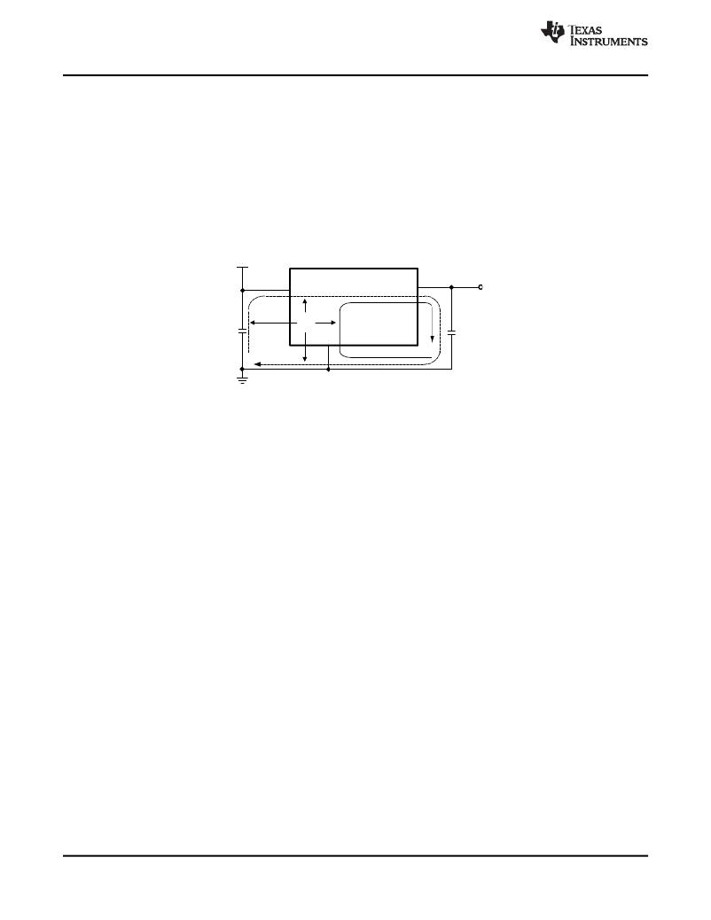
�V� IN�
�VIN�
�LMZ14201�
�VOUT�
�V� O�
�High�
�C� in1�
�Loop� 1�
�di/dt�
�GND�
�Loop� 2�
�C� O1�
�1.� Minimize� area� of� switched� current� loops.�
�From� an� EMI� reduction� standpoint,� it� is� imperative� to� minimize� the� high� di/dt� paths� during� PC� board� layout.� The�
�high� current� loops� that� do� not� overlap� have� high� di/dt� content� that� will� cause� observable� high� frequency� noise� on�
�the� output� pin� if� the� input� capacitor� (Cin1)� is� placed� at� a� distance� away� from� the� LMZ14201.� Therefore� place� C� IN1�
�as� close� as� possible� to� the� LMZ14201� VIN� and� GND� exposed� pad.� This� will� minimize� the� high� di/dt� area� and�
�reduce� radiated� EMI.� Additionally,� grounding� for� both� the� input� and� output� capacitor� should� consist� of� a� localized�
�top� side� plane� that� connects� to� the� GND� exposed� pad� (EP).�
�2.� Have� a� single� point� ground.�
�The� ground� connections� for� the� feedback,� soft-start,� and� enable� components� should� be� routed� to� the� GND� pin� of�
�the� device.� This� prevents� any� switched� or� load� currents� from� flowing� in� the� analog� ground� traces.� If� not� properly�
�handled,� poor� grounding� can� result� in� degraded� load� regulation� or� erratic� output� voltage� ripple� behavior.� Provide�
�the� single� point� ground� connection� from� pin� 4� to� EP.�
�3.� Minimize� trace� length� to� the� FB� pin.�
�Both� feedback� resistors,� R� FBT� and� R� FBB� ,� and� the� feed� forward� capacitor� C� FF� ,� should� be� located� close� to� the� FB�
�pin.� Since� the� FB� node� is� high� impedance,� maintain� the� copper� area� as� small� as� possible.� The� trace� are� from�
�R� FBT� ,� R� FBB� ,� and� C� FF� should� be� routed� away� from� the� body� of� the� LMZ14201� to� minimize� noise.�
�4.� Make� input� and� output� bus� connections� as� wide� as� possible.�
�This� reduces� any� voltage� drops� on� the� input� or� output� of� the� converter� and� maximizes� efficiency.� To� optimize�
�voltage� accuracy� at� the� load,� ensure� that� a� separate� feedback� voltage� sense� trace� is� made� to� the� load.� Doing� so�
�will� correct� for� voltage� drops� and� provide� optimum� output� accuracy.�
�5.� Provide� adequate� device� heat-sinking.�
�Use� an� array� of� heat-sinking� vias� to� connect� the� exposed� pad� to� the� ground� plane� on� the� bottom� PCB� layer.� If�
�the� PCB� has� a� plurality� of� copper� layers,� these� thermal� vias� can� also� be� employed� to� make� connection� to� inner�
�layer� heat-spreading� ground� planes.� For� best� results� use� a� 6� x� 6� via� array� with� minimum� via� diameter� of� 8mils�
�thermal� vias� spaced� 59mils� (1.5� mm).� Ensure� enough� copper� area� is� used� for� heat-sinking� to� keep� the� junction�
�temperature� below� 125°C.�
�16�
�Submit� Documentation� Feedback�
�Product� Folder� Links:� LMZ14201�
�Copyright� ?� 2010–2013,� Texas� Instruments� Incorporated�
�相关PDF资料 |
PDF描述 |
|---|---|
| VE-26T-CY-F2 | CONVERTER MOD DC/DC 6.5V 50W |
| 180-062-113R021 | CONN DB62 MALE HD DIP SLD NICKEL |
| VI-J3D-IZ | CONVERTER MOD DC/DC 85V 25W |
| SWS1005 | PWR SUP 5V 20A SNG OUTPUT |
| VI-J3B-IZ | CONVERTER MOD DC/DC 95V 25W |
相关代理商/技术参数 |
参数描述 |
|---|---|
| LMZ14202 | 制造商:NSC 制造商全称:National Semiconductor 功能描述:2A SIMPLE SWITCHER? Power Module with 42V Maximum Input Voltage |
| LMZ14202_1 | 制造商:NSC 制造商全称:National Semiconductor 功能描述:2A SIMPLE SWITCHER?? Power Module with 42V Maximum Input Voltage |
| LMZ14202_11 | 制造商:NSC 制造商全称:National Semiconductor 功能描述:2A SIMPLE SWITCHER? Power Module with 42V Maximum Input Voltage |
| LMZ14202EVAL/NOPB | 功能描述:电源管理IC开发工具 LMZ14202EVAL BOARD RoHS:否 制造商:Maxim Integrated 产品:Evaluation Kits 类型:Battery Management 工具用于评估:MAX17710GB 输入电压: 输出电压:1.8 V |
| LMZ14202EXT | 制造商:TI 制造商全称:Texas Instruments 功能描述:2A SIMPLE SWITCHER?? Power Module with 42V Maximum Input Voltage for Military and Rugged Applications |
发布紧急采购,3分钟左右您将得到回复。