- 您现在的位置:买卖IC网 > PDF目录44716 > LNK603GG-TL (POWER INTEGRATIONS INC) SPECIALTY ANALOG CIRCUIT, PDSO8 PDF资料下载
参数资料
| 型号: | LNK603GG-TL |
| 厂商: | POWER INTEGRATIONS INC |
| 元件分类: | 模拟信号调理 |
| 英文描述: | SPECIALTY ANALOG CIRCUIT, PDSO8 |
| 封装: | GREEN, PLASTIC, SMD-8 |
| 文件页数: | 15/20页 |
| 文件大小: | 722K |
| 代理商: | LNK603GG-TL |
Rev. C 06/08
4
LNK603-606/613-616
www.powerint.com
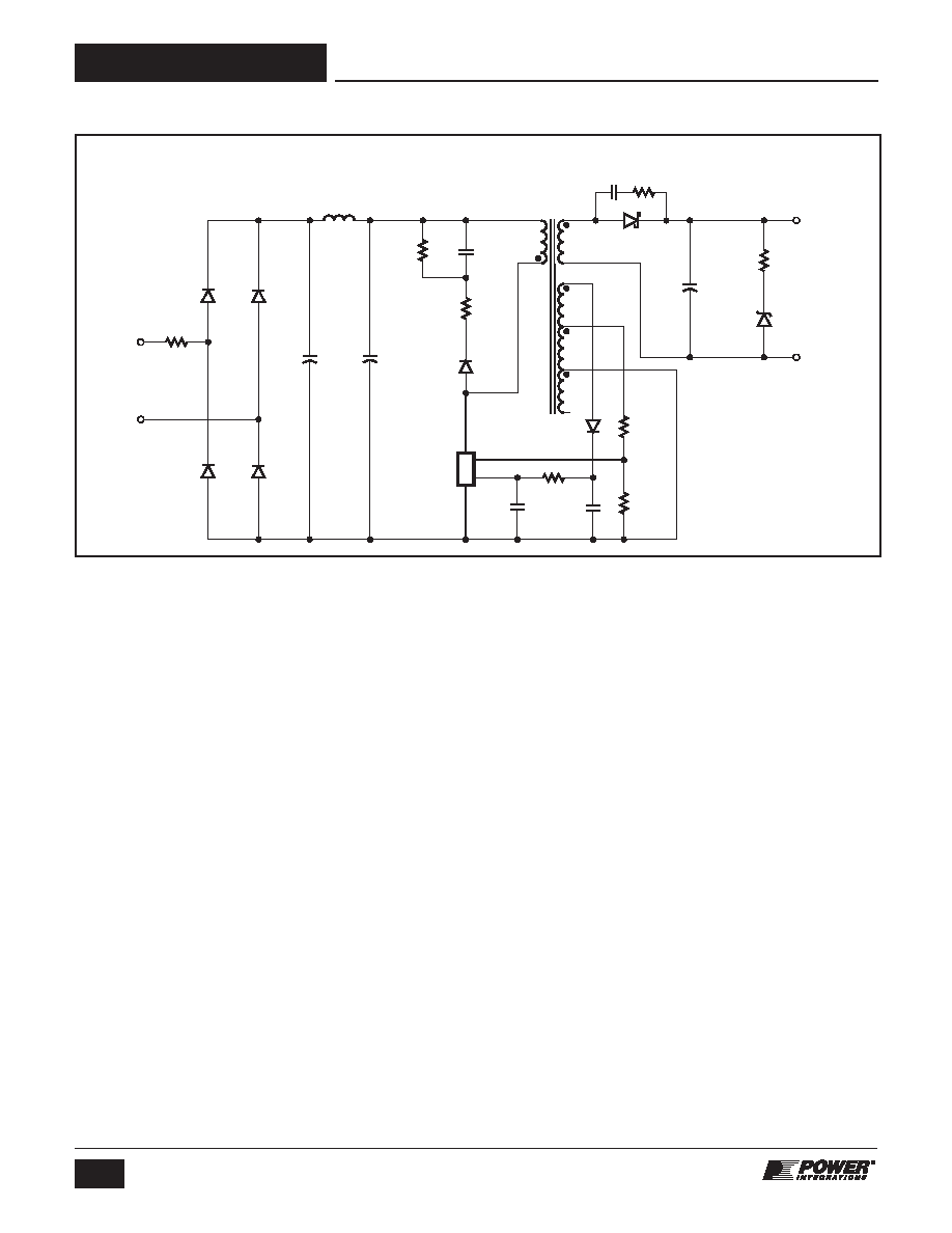
Applications Example
Circuit Description
This circuit shown in Figure 4 is congured as a primary-side
regulated yback power supply utilizing the LNK613DG. With
an average efciency of 74% and <40 mW no-load input power
this design easily exceeds the most stringent current energy
efciency requirements.
Input Filter
AC input power is rectied by diodes D1 through D4. The
rectied DC is ltered by the bulk storage capacitors C1 and
C2. Inductor L1, C1 and C2 form a pi (π) lter, which attenuates
conducted differential-mode EMI noise. This conguration
along with Power Integrations transformer E-shield technology
allow this design to meet EMI standard EN55022 class B with
good margin without requiring a Y capacitor, even with the
output connected to safety earth ground. Fusible resistor RF1
provides protection against catastrophic failure. This should be
suitably rated (typically a wire wound type) to withstand the
instantaneous dissipation while the input capacitors charge
when rst connected to the AC line.
LNK 613 Primary
The LNK613DG device (U1) incorporates the power switching
device, oscillator, CC/CV control engine, startup, and protection
functions. The integrated 700 V MOSFET provides a large drain
voltage margin in universal input AC applications, increasing
reliability and also reducing the output diode voltage stress by
allowing a greater transformer turns ratio. The device is
completely self-powered from the BYPASS pin and decoupling
capacitor C4. For the LNK61X devices, the bypass capacitor
value also selects the amount of output cable voltage drop
compensation. A 1 μF value selects the standard compensation.
A 10 μF value selects the enhanced compensation. Table 2
shows the amount of compensation for each device and
bypass capacitor value. The LNK60x devices do not provide
cable drop compensation.
The optional bias supply formed by D6 and C5 provides the
operating current for U1 via resistor R4. This reduces the no-
load consumption from ~200 mW to <40 mW and also
increases light load efciency.
The rectied and ltered input voltage is applied to one side of
the primary winding of T1. The other side of the transformer’s
primary winding is driven by the integrated MOSFET in U1. The
leakage inductance drain voltage spike is limited by an RCD-R
clamp consisting of D5, R2, R3, and C3.
Output Rectication
The secondary of the transformer is rectied by D7, a 1 A, 40 V
Schottky barrier type for higher efciency, and ltered by C7. If
lower efciency is acceptable then this can be replaced with a
1 A PN junction diode for lower cost. In this application C7 was
sized to meet the required output voltage ripple specication
without requiring a post LC lter. To meet battery self discharge
requirement the pre-load resistor has been replaced with a
series resistor and Zener network (R8 and VR1). However in
designs where this is not a requirement a standard 1 kΩ
resistor can be used.
Output Regulation
The LNK613 regulates the output using ON/OFF control in the
constant voltage (CV) regulation region of the output character-
Figure 4.
Energy Efcient USB Charger Power Supply (74% Average Efciency, <40 mW No-load Input Power).
PI-5111-050808
D
S
FB
BP
R2
470 k
R3
300
R5
13 k
1%
R7
200
R8
200
R6
8.87 k
1%
R4
6.2 k
RF1
8.2
2 W
D5
1N4007
D7
SS14
D6
LL4148
VR1
2MM5230B-7
4.7 V
D1
1N4007
D2
1N4007
D3
1N4007
D4
1N4007
T1
EE16
510
8
1
2
4
NC
3
C7
680 F
10 V
C6
1 nF
100 V
C1
4.7 F
400 V
C2
4.7 F
400 V
C4
1 F
25 V
C5
10 F
16 V
L1
1.5 mH
C3
820 pF
1 kV
DC
Output
5 V, 555 mA
U1
LNK613DG
LinkSwitch-II
AC
Input
相关PDF资料 |
PDF描述 |
|---|---|
| LNK604GG | SPECIALTY ANALOG CIRCUIT, PDSO8 |
| LNK616GG | SPECIALTY ANALOG CIRCUIT, PDSO8 |
| LNK605DG | SPECIALTY ANALOG CIRCUIT, PDSO8 |
| LNK604DG | SPECIALTY ANALOG CIRCUIT, PDSO8 |
| LNK606GG | SPECIALTY ANALOG CIRCUIT, PDSO8 |
相关代理商/技术参数 |
参数描述 |
|---|---|
| LNK603PG | 功能描述:交流/直流开关转换器 85-265 VAC 2.5W LinkSwitch II RoHS:否 制造商:STMicroelectronics 输出电压:800 V 输入/电源电压(最大值):23.5 V 输入/电源电压(最小值):11.5 V 开关频率:115 kHz 电源电流:1.6 mA 工作温度范围:- 40 C to + 150 C 安装风格:SMD/SMT 封装 / 箱体:SSO-10 封装:Reel |
| LNK603PG-TL | 制造商:POWERINT 制造商全称:Power Integrations, Inc. 功能描述:Energy-Efficient, Accurate CV/CC Switcher for Adapters and Chargers |
| LNK604 | 制造商:POWERINT 制造商全称:Power Integrations, Inc. 功能描述:Energy-Efficient, Accurate CV/CC Switcher for Adapters and Chargers |
| LNK604DG | 功能描述:交流/直流开关转换器 3.5 W (85-265 VAC) RoHS:否 制造商:STMicroelectronics 输出电压:800 V 输入/电源电压(最大值):23.5 V 输入/电源电压(最小值):11.5 V 开关频率:115 kHz 电源电流:1.6 mA 工作温度范围:- 40 C to + 150 C 安装风格:SMD/SMT 封装 / 箱体:SSO-10 封装:Reel |
| LNK604DG-TL | 功能描述:交流/直流开关转换器 85-265 VAC 3.5W LinkSwitch II RoHS:否 制造商:STMicroelectronics 输出电压:800 V 输入/电源电压(最大值):23.5 V 输入/电源电压(最小值):11.5 V 开关频率:115 kHz 电源电流:1.6 mA 工作温度范围:- 40 C to + 150 C 安装风格:SMD/SMT 封装 / 箱体:SSO-10 封装:Reel |
发布紧急采购,3分钟左右您将得到回复。