- 您现在的位置:买卖IC网 > PDF目录44716 > LNK603GG-TL (POWER INTEGRATIONS INC) SPECIALTY ANALOG CIRCUIT, PDSO8 PDF资料下载
参数资料
| 型号: | LNK603GG-TL |
| 厂商: | POWER INTEGRATIONS INC |
| 元件分类: | 模拟信号调理 |
| 英文描述: | SPECIALTY ANALOG CIRCUIT, PDSO8 |
| 封装: | GREEN, PLASTIC, SMD-8 |
| 文件页数: | 17/20页 |
| 文件大小: | 722K |
| 代理商: | LNK603GG-TL |
Rev. C 06/08
6
LNK603-606/613-616
www.powerint.com
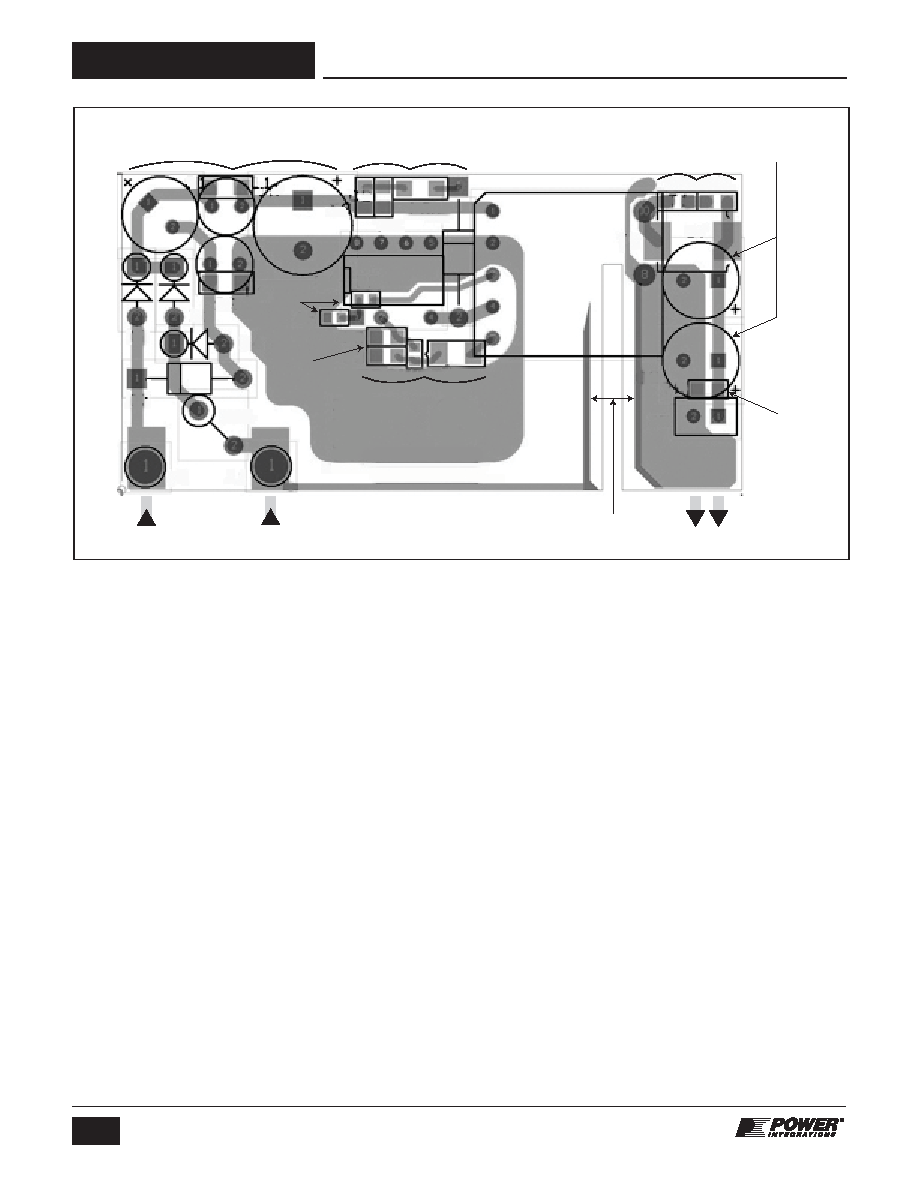
Secondary Loop Area
To minimize leakage inductance and EMI the area of the loop
connecting the secondary winding, the output diode and the
output lter capacitor should be minimized. In addition,
sufcient copper area should be provided at the anode and
cathode terminal of the diode for heatsinking. A larger area is
preferred at the quiet cathode terminal. A large anode area can
increase high frequency radiated EMI.
Electrostatic Discharge Spark Gap
An trace is placed along the isolation barrier to form one
electrode of a spark gap. The other electrode on the secondary
is formed by the output return node. The spark gap directs
ESD energy from the secondary back to the AC input. The
trace from the AC input to the spark gap electrode should be
spaced away from other traces to prevent unwanted arcing
occurring and possible circuit damage.
Drain Clamp Optimization
LinkSwitch-II senses the feedback winding on the primary side
to regulate the output. The voltage that appears on the feed-
back winding is a reection of the secondary winding voltage
while the internal MOSFET is off. Therefore any leakage
inductance induced ringing can affect output regulation.
Optimizing the drain clamp to minimize the high frequency
ringing will give the best regulation. Figure 6 shows the desired
drain voltage waveform compared to Figure 7 with a large
undershoot due to the leakage inductance induced ring. This
will reduce the output voltage regulation performance. To
Figure 5.
PCB Layout Example Showing 5.1 W Design using P Package.
reduce this adjust the value of the resistor in series with the
clamp diode.
Addition of a bias circuit for higher light load efciency
and lower no load input power consumption.
The addition of a bias circuit can decrease the no load input
power from ~200 mW down to less than 30 mW at 230 VAC
input. Light load efciency also increases which may avoid the
need to use a Schottky barrier vs PN junction output diode
while still meeting average efciency requirements.
The power supply schematic shown in Figure 4 has the bias
circuit incorporated. Diode D6, C5 and R4 form the bias circuit.
As the output voltage is less than 8 V, an additional transformer
winding is needed, AC stacked on top of the feedback winding.
This provides a high enough voltage to supply the BYPASS pin
even during low switching frequency operation at no-load.
In Figure 4 the additional bias winding (from pin 2 to pin 1) is
stacked on top of the feedback winding (pin 4 to pin 2). Diode
D6 recties the output and C5 is the lter capacitor. A 10 uF
capacitor is recommended to hold up the bias voltage at low
switching frequencies. The capacitor type is not critical but the
voltage rating should be above the maximum value of V
BIAS.
The recommended current into the BP pin is equal to IC supply
current (~0.5 mA). The value of R4 is calculated according to
(V
BIAS – VBP)/IS2, where VBIAS (10 V typ.) is the voltage across C5,
I
S2 (0.5 mA typ.) is the IC supply current and VBP (6.2 V typ.) is
DC
Output
PI-5110-050508
R5
C4
C5
C3
R4
D5
D3
R3
R1
C2
R1
C1
R6
R2
L2
D4
D2
D1
U1
D3
RF1
D7
T1
R8
C6
C7
C8
R9
Output Filter
Capacitors
Input Stage
Primary Clamp
Output
Diode Snubber
Preload
Resistor
Spark
Gap
Bypass
Capacitor
Feedback
Resistors
Bypass Supply
Components
AC
Input
SS
S
BP
D
FB
LinkSwitch-II
相关PDF资料 |
PDF描述 |
|---|---|
| LNK604GG | SPECIALTY ANALOG CIRCUIT, PDSO8 |
| LNK616GG | SPECIALTY ANALOG CIRCUIT, PDSO8 |
| LNK605DG | SPECIALTY ANALOG CIRCUIT, PDSO8 |
| LNK604DG | SPECIALTY ANALOG CIRCUIT, PDSO8 |
| LNK606GG | SPECIALTY ANALOG CIRCUIT, PDSO8 |
相关代理商/技术参数 |
参数描述 |
|---|---|
| LNK603PG | 功能描述:交流/直流开关转换器 85-265 VAC 2.5W LinkSwitch II RoHS:否 制造商:STMicroelectronics 输出电压:800 V 输入/电源电压(最大值):23.5 V 输入/电源电压(最小值):11.5 V 开关频率:115 kHz 电源电流:1.6 mA 工作温度范围:- 40 C to + 150 C 安装风格:SMD/SMT 封装 / 箱体:SSO-10 封装:Reel |
| LNK603PG-TL | 制造商:POWERINT 制造商全称:Power Integrations, Inc. 功能描述:Energy-Efficient, Accurate CV/CC Switcher for Adapters and Chargers |
| LNK604 | 制造商:POWERINT 制造商全称:Power Integrations, Inc. 功能描述:Energy-Efficient, Accurate CV/CC Switcher for Adapters and Chargers |
| LNK604DG | 功能描述:交流/直流开关转换器 3.5 W (85-265 VAC) RoHS:否 制造商:STMicroelectronics 输出电压:800 V 输入/电源电压(最大值):23.5 V 输入/电源电压(最小值):11.5 V 开关频率:115 kHz 电源电流:1.6 mA 工作温度范围:- 40 C to + 150 C 安装风格:SMD/SMT 封装 / 箱体:SSO-10 封装:Reel |
| LNK604DG-TL | 功能描述:交流/直流开关转换器 85-265 VAC 3.5W LinkSwitch II RoHS:否 制造商:STMicroelectronics 输出电压:800 V 输入/电源电压(最大值):23.5 V 输入/电源电压(最小值):11.5 V 开关频率:115 kHz 电源电流:1.6 mA 工作温度范围:- 40 C to + 150 C 安装风格:SMD/SMT 封装 / 箱体:SSO-10 封装:Reel |
发布紧急采购,3分钟左右您将得到回复。