- 您现在的位置:买卖IC网 > PDF目录22121 > LNK613DG (Power Integrations)IC OFFLINE SWIT CV/CC HV 8SOIC PDF资料下载
参数资料
| 型号: | LNK613DG |
| 厂商: | Power Integrations |
| 文件页数: | 4/18页 |
| 文件大小: | 0K |
| 描述: | IC OFFLINE SWIT CV/CC HV 8SOIC |
| 应用说明: | LinkSwitch-II Family, Appl Note AN-44 |
| 产品培训模块: | LinkSwitch-II Overview |
| 特色产品: | LinkSwitch?-II Product Family |
| 标准包装: | 100 |
| 输出隔离: | 隔离 |
| 频率范围: | 58kHz ~ 72kHz |
| 输出电压: | 700V |
| 功率(瓦特): | 3.3W |
| 工作温度: | -40°C ~ 150°C |
| 封装/外壳: | 8-SOIC(0.154",3.90mm 宽)7 引线 |
| 供应商设备封装: | SO-8C |
| 包装: | 管件 |
| 产品目录页面: | 1202 (CN2011-ZH PDF) |
| 配用: | 596-1235-ND - KIT REF DESIGN LINKSWITCH 2 |
| 其它名称: | 596-1222-5 |
��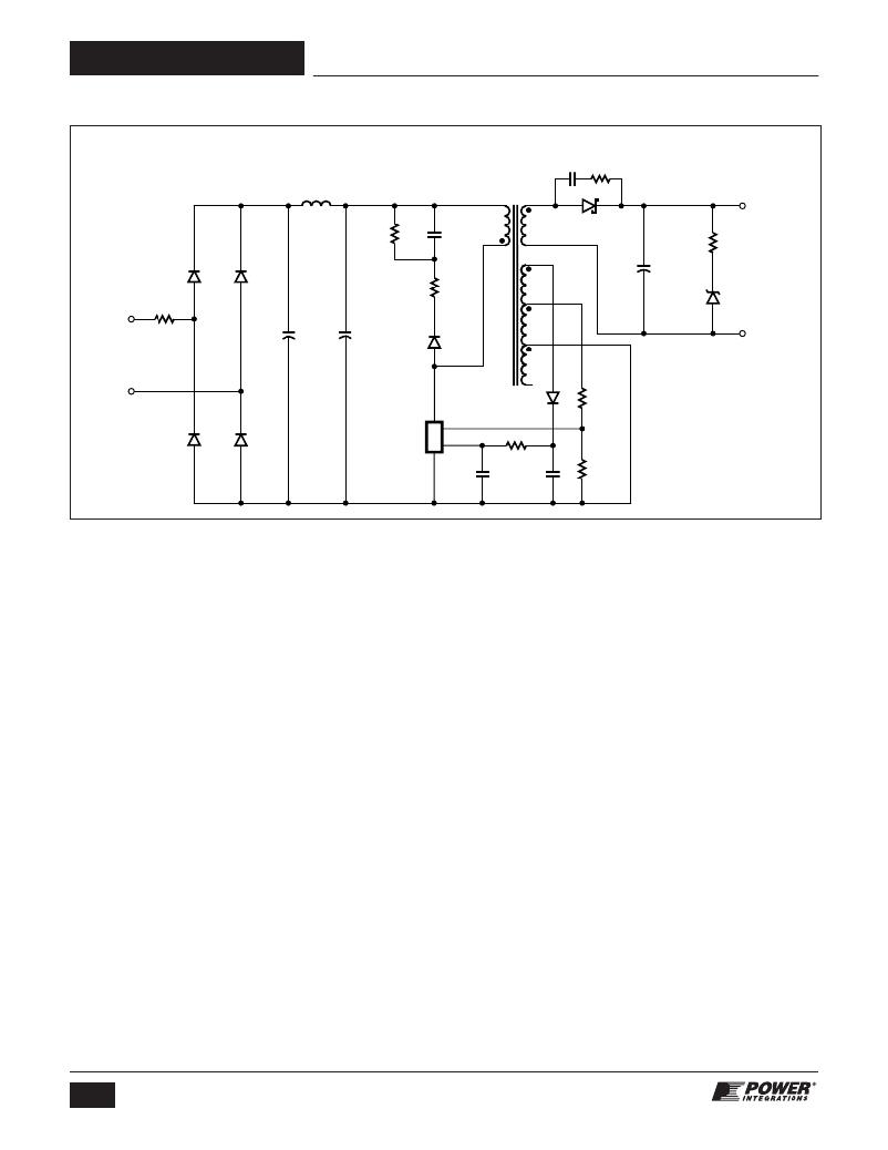 �
�
�LNK603-606/613-616�
�Applications� Example�
�C6�
�1� nF� R7�
�100� V� 200� ?�
�L1�
�1.5� mH�
�5�
�T1�
�EE16�
�10�
�5� V,� 555� mA�
�820� pF� 3�
�AC�
�Input�
�RF1�
�8.2� ?�
�2W�
�D1�
�1N4007�
�D2�
�1N4007�
�C1�
�4.7� μ� F�
�400� V�
�R2�
�470� k� ?�
�C2�
�4.7� μ� F�
�400� V�
�R3�
�300� ?�
�D5�
�1N4007�
�C3�
�1� kV�
�8�
�1�
�2�
�4�
�D7�
�SS14�
�C7�
�680� μ� F�
�10� V�
�R8�
�200� ?�
�VR1�
�2MM5230B-7�
�4.7� V�
�DC�
�Output�
�D3�
�1N4007�
�D4�
�1N4007�
�D�
�LinkSwitch-II�
�U1�
�LNK613DG�
�FB�
�NC�
�D6�
�LL4148�
�R5�
�13� k� ?�
�1%�
�BP�
�S�
�C4�
�1� μ� F�
�25� V�
�R4�
�6.2� k� ?� C5�
�10� μ� F�
�16� V�
�R6�
�8.87� k� ?�
�1%�
�PI-5111-050808�
�Figure� 4.�
�Energy� Efficient� USB� Charger� Power� Supply� (74%� Average� Efficiency,� <30� mW� No-load� Input� Power).�
�Circuit� Description�
�This� circuit� shown� in� Figure� 4� is� configured� as� a� primary-side�
�regulated� flyback� power� supply� utilizing� the� LNK613DG.� With�
�an� average� efficiency� of� 74%� and� <30� mW� no-load� input� power�
�this� design� easily� exceeds� the� most� stringent� current� energy�
�efficiency� requirements.�
�Input� Filter�
�AC� input� power� is� rectified� by� diodes� D1� through� D4.� The�
�rectified� DC� is� filtered� by� the� bulk� storage� capacitors� C1� and�
�C2.� Inductor� L1,� C1� and� C2� form� a� pi� (π)� filter,� which� attenuates�
�conducted� differential-mode� EMI� noise.� This� configuration�
�along� with� Power� Integrations� transformer� E-shield� ?� technology�
�allow� this� design� to� meet� EMI� standard� EN55022� class� B� with�
�good� margin� without� requiring� a� Y� capacitor,� even� with� the�
�output� connected� to� safety� earth� ground.� Fusible� resistor� RF1�
�provides� protection� against� catastrophic� failure.� This� should� be�
�suitably� rated� (typically� a� wire� wound� type)� to� withstand� the�
�instantaneous� dissipation� while� the� input� capacitors� charge�
�when� first� connected� to� the� AC� line.�
�LNK� 613� Primary�
�The� LNK613DG� device� (U1)� incorporates� the� power� switching�
�device,� oscillator,� CC/CV� control� engine,� startup,� and� protection�
�functions.� The� integrated� 700� V� MOSFET� provides� a� large� drain�
�voltage� margin� in� universal� input� AC� applications,� increasing�
�reliability� and� also� reducing� the� output� diode� voltage� stress� by�
�allowing� a� greater� transformer� turns� ratio.� The� device� is�
�completely� self-powered� from� the� BYPASS� pin� and� decoupling�
�capacitor� C4.� For� the� LNK61X� devices,� the� bypass� capacitor�
�value� also� selects� the� amount� of� output� cable� voltage� drop�
�4�
�Rev.� F� 01/10�
�compensation.� A� 1� m� F� value� selects� the� standard� compensation.�
�A� 10� m� F� value� selects� the� enhanced� compensation.� Table� 2�
�shows� the� amount� of� compensation� for� each� device� and�
�bypass� capacitor� value.� The� LNK60x� devices� do� not� provide�
�cable� drop� compensation.�
�The� optional� bias� supply� formed� by� D6� and� C5� provides� the�
�operating� current� for� U1� via� resistor� R4.� This� reduces� the�
�no-load� consumption� from� ~200� mW� to� <30� mW� and� also�
�increases� light� load� efficiency.�
�The� rectified� and� filtered� input� voltage� is� applied� to� one� side� of�
�the� primary� winding� of� T1.� The� other� side� of� the� transformer’s�
�primary� winding� is� driven� by� the� integrated� MOSFET� in� U1.� The�
�leakage� inductance� drain� voltage� spike� is� limited� by� an� RCD-R�
�clamp� consisting� of� D5,� R2,� R3,� and� C3.�
�Output� Rectification�
�The� secondary� of� the� transformer� is� rectified� by� D7,� a� 1� A,� 40� V�
�Schottky� barrier� type� for� higher� efficiency,� and� filtered� by� C7.� If�
�lower� efficiency� is� acceptable� then� this� can� be� replaced� with� a�
�1� A� PN� junction� diode� for� lower� cost.� In� this� application� C7� was�
�sized� to� meet� the� required� output� voltage� ripple� specification�
�without� requiring� a� post� LC� filter.� To� meet� battery� self� discharge�
�requirement� the� pre-load� resistor� has� been� replaced� with� a�
�series� resistor� and� Zener� network� (R8� and� VR1).� However� in�
�designs� where� this� is� not� a� requirement� a� standard� 1� k� W�
�resistor� can� be� used.�
�Output� Regulation�
�The� LNK613� regulates� the� output� using� ON/OFF� control� in� the�
�constant� voltage� (CV)� regulation� region� of� the� output� character-�
�www.powerint.com�
�相关PDF资料 |
PDF描述 |
|---|---|
| LTC1421CG#PBF | IC CONTROLLER HOT SWAP 24-SSOP |
| R2D12-2424/P | CONV DC/DC 2W +/-24VOUT SMD |
| 7-530666-6 | CONN LOW PRO 22 POS 156X200C/L |
| LTC1421ISW#TR | IC CONTROLLER HOTSWAP ADJ 24SOIC |
| LA4032V-75TN48E | IC CPLD 32MACROCELLS 48TQFP |
相关代理商/技术参数 |
参数描述 |
|---|---|
| LNK613DG-TL | 功能描述:交流/直流开关转换器 85-265 VAC 2.5W LinkSwitch II RoHS:否 制造商:STMicroelectronics 输出电压:800 V 输入/电源电压(最大值):23.5 V 输入/电源电压(最小值):11.5 V 开关频率:115 kHz 电源电流:1.6 mA 工作温度范围:- 40 C to + 150 C 安装风格:SMD/SMT 封装 / 箱体:SSO-10 封装:Reel |
| LNK613PG | 功能描述:交流/直流开关转换器 85-265 VAC 2.5W LinkSwitch II RoHS:否 制造商:STMicroelectronics 输出电压:800 V 输入/电源电压(最大值):23.5 V 输入/电源电压(最小值):11.5 V 开关频率:115 kHz 电源电流:1.6 mA 工作温度范围:- 40 C to + 150 C 安装风格:SMD/SMT 封装 / 箱体:SSO-10 封装:Reel |
| LNK613PG-TL | 制造商:POWERINT 制造商全称:Power Integrations, Inc. 功能描述:Energy-Efficient, Accurate CV/CC Switcher for Adapters and Chargers |
| LNK614DG | 功能描述:交流/直流开关转换器 3.5 W (85-265 VAC) RoHS:否 制造商:STMicroelectronics 输出电压:800 V 输入/电源电压(最大值):23.5 V 输入/电源电压(最小值):11.5 V 开关频率:115 kHz 电源电流:1.6 mA 工作温度范围:- 40 C to + 150 C 安装风格:SMD/SMT 封装 / 箱体:SSO-10 封装:Reel |
| LNK614DG-TL | 功能描述:交流/直流开关转换器 85-265 VAC 3.5W LinkSwitch II RoHS:否 制造商:STMicroelectronics 输出电压:800 V 输入/电源电压(最大值):23.5 V 输入/电源电压(最小值):11.5 V 开关频率:115 kHz 电源电流:1.6 mA 工作温度范围:- 40 C to + 150 C 安装风格:SMD/SMT 封装 / 箱体:SSO-10 封装:Reel |
发布紧急采购,3分钟左右您将得到回复。