- 您现在的位置:买卖IC网 > PDF目录22121 > LNK613DG (Power Integrations)IC OFFLINE SWIT CV/CC HV 8SOIC PDF资料下载
参数资料
| 型号: | LNK613DG |
| 厂商: | Power Integrations |
| 文件页数: | 6/18页 |
| 文件大小: | 0K |
| 描述: | IC OFFLINE SWIT CV/CC HV 8SOIC |
| 应用说明: | LinkSwitch-II Family, Appl Note AN-44 |
| 产品培训模块: | LinkSwitch-II Overview |
| 特色产品: | LinkSwitch?-II Product Family |
| 标准包装: | 100 |
| 输出隔离: | 隔离 |
| 频率范围: | 58kHz ~ 72kHz |
| 输出电压: | 700V |
| 功率(瓦特): | 3.3W |
| 工作温度: | -40°C ~ 150°C |
| 封装/外壳: | 8-SOIC(0.154",3.90mm 宽)7 引线 |
| 供应商设备封装: | SO-8C |
| 包装: | 管件 |
| 产品目录页面: | 1202 (CN2011-ZH PDF) |
| 配用: | 596-1235-ND - KIT REF DESIGN LINKSWITCH 2 |
| 其它名称: | 596-1222-5 |
�� �
�
�LNK603-606/613-616�
�Input� Stage�
�Primary� Clamp�
�Output� Filter�
�Output� Capacitors�
�Diode� Snubber�
�C1�
�R1�
�C2�
�T1�
�R8�
�C6�
�R3�
�S�
�S�
�C3�
�S�
�R4�
�S�
�D5�
�D7�
�R1�
�LinkSwitch-II�
�L2�
�Resistors�
�D1�
�R2�
�U1�
�Feedback�
�R6�
�R5�
�FB�
�BP�
�D�
�C7�
�D2�
�D4�
�C4�
�D3�
�RF1�
�Bypass�
�Capacitor�
�C5�
�D3�
�Bypass� Supply�
�Components�
�C8�
�R9�
�Preload�
�Resistor�
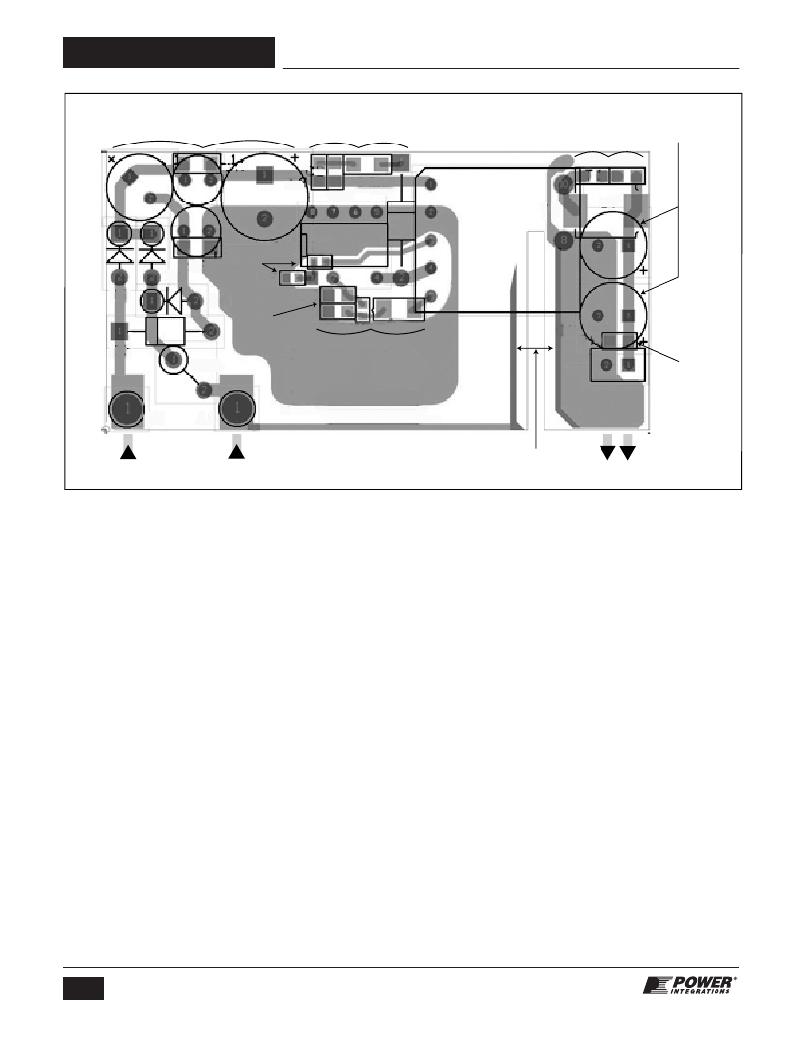
�Figure� 5.�
�AC�
�Input�
�PCB� Layout� Example� Showing� 5.1� W� Design� Using� P� Package.�
�Spark�
�Gap�
�DC�
�Output�
�PI-5110-050508�
�Secondary� Loop� Area�
�To� minimize� leakage� inductance� and� EMI� the� area� of� the� loop�
�connecting� the� secondary� winding,� the� output� diode� and� the�
�output� filter� capacitor� should� be� minimized.� In� addition,�
�sufficient� copper� area� should� be� provided� at� the� anode� and�
�cathode� terminal� of� the� diode� for� heatsinking.� A� larger� area� is�
�preferred� at� the� quiet� cathode� terminal.� A� large� anode� area� can�
�increase� high� frequency� radiated� EMI.�
�Electrostatic� Discharge� Spark� Gap�
�An� trace� is� placed� along� the� isolation� barrier� to� form� one�
�electrode� of� a� spark� gap.� The� other� electrode� on� the� secondary�
�is� formed� by� the� output� return� node.� The� spark� gap� directs�
�ESD� energy� from� the� secondary� back� to� the� AC� input.� The�
�trace� from� the� AC� input� to� the� spark� gap� electrode� should� be�
�spaced� away� from� other� traces� to� prevent� unwanted� arcing�
�occurring� and� possible� circuit� damage.�
�Drain� Clamp� Optimization�
�LinkSwitch-II� senses� the� feedback� winding� on� the� primary� side�
�to� regulate� the� output.� The� voltage� that� appears� on� the� feed-�
�back� winding� is� a� reflection� of� the� secondary� winding� voltage�
�while� the� internal� MOSFET� is� off.� Therefore� any� leakage�
�inductance� induced� ringing� can� affect� output� regulation.� Optimizing�
�the� drain� clamp� to� minimize� the� high� frequency� ringing� will� give�
�the� best� regulation.� Figure� 6� shows� the� desired� drain� voltage�
�waveform� compared� to� Figure� 7� with� a� large� undershoot� due� to�
�the� leakage� inductance� induced� ring.� This� will� reduce� the�
�output� voltage� regulation� performance.� To� reduce� this� adjust�
�the� value� of� the� resistor� in� series� with� the� clamp� diode.�
�6�
�Rev.� F� 01/10�
�Addition� of� a� Bias� Circuit� for� Higher� Light� Load� Efficiency�
�and� Lower� No-load� Input� Power� Consumption.�
�The� addition� of� a� bias� circuit� can� decrease� the� no-load� input�
�power� from� ~200� mW� down� to� less� than� 30� mW� at� 230� VAC�
�input.� Light� load� efficiency� also� increases� which� may� avoid� the�
�need� to� use� a� Schottky� barrier� vs� PN� junction� output� diode�
�while� still� meeting� average� efficiency� requirements.�
�The� power� supply� schematic� shown� in� Figure� 4� has� the� bias�
�circuit� incorporated.� Diode� D6,� C5� and� R4� form� the� bias� circuit.�
�As� the� output� voltage� is� less� than� 8� V,� an� additional� transformer�
�winding� is� needed,� AC� stacked� on� top� of� the� feedback� winding.�
�This� provides� a� high� enough� voltage� to� supply� the� BYPASS� pin�
�even� during� low� switching� frequency� operation� at� no-load.�
�In� Figure� 4� the� additional� bias� winding� (from� pin� 2� to� pin� 1)� is�
�stacked� on� top� of� the� feedback� winding� (pin� 4� to� pin� 2).� Diode�
�D6� rectifies� the� output� and� C5� is� the� filter� capacitor.� A� 10� uF�
�capacitor� is� recommended� to� hold� up� the� bias� voltage� at� low�
�switching� frequencies.� The� capacitor� type� is� not� critical� but� the�
�voltage� rating� should� be� above� the� maximum� value� of� V� BIAS� .�
�The� recommended� current� into� the� BYPASS� pin� is� equal� to� IC�
�supply� current� (~0.5� mA)� at� the� minimum� bias� winding� voltage.�
�The� BYPASS� pin� current� should� not� exceed� 3� mA� at� the� maximum�
�bias� winding� voltage.� The� value� of� R4� is� calculated� according� to�
�(V� BIAS� –� V� BP� )/I� S2� ,� where� V� BIAS� (10� V� typ.)� is� the� voltage� across� C5,� I� S2�
�(0.5� mA� typ.)� is� the� IC� supply� current� and� V� BP� (6.2� V� typ.)� is� the�
�www.powerint.com�
�相关PDF资料 |
PDF描述 |
|---|---|
| LTC1421CG#PBF | IC CONTROLLER HOT SWAP 24-SSOP |
| R2D12-2424/P | CONV DC/DC 2W +/-24VOUT SMD |
| 7-530666-6 | CONN LOW PRO 22 POS 156X200C/L |
| LTC1421ISW#TR | IC CONTROLLER HOTSWAP ADJ 24SOIC |
| LA4032V-75TN48E | IC CPLD 32MACROCELLS 48TQFP |
相关代理商/技术参数 |
参数描述 |
|---|---|
| LNK613DG-TL | 功能描述:交流/直流开关转换器 85-265 VAC 2.5W LinkSwitch II RoHS:否 制造商:STMicroelectronics 输出电压:800 V 输入/电源电压(最大值):23.5 V 输入/电源电压(最小值):11.5 V 开关频率:115 kHz 电源电流:1.6 mA 工作温度范围:- 40 C to + 150 C 安装风格:SMD/SMT 封装 / 箱体:SSO-10 封装:Reel |
| LNK613PG | 功能描述:交流/直流开关转换器 85-265 VAC 2.5W LinkSwitch II RoHS:否 制造商:STMicroelectronics 输出电压:800 V 输入/电源电压(最大值):23.5 V 输入/电源电压(最小值):11.5 V 开关频率:115 kHz 电源电流:1.6 mA 工作温度范围:- 40 C to + 150 C 安装风格:SMD/SMT 封装 / 箱体:SSO-10 封装:Reel |
| LNK613PG-TL | 制造商:POWERINT 制造商全称:Power Integrations, Inc. 功能描述:Energy-Efficient, Accurate CV/CC Switcher for Adapters and Chargers |
| LNK614DG | 功能描述:交流/直流开关转换器 3.5 W (85-265 VAC) RoHS:否 制造商:STMicroelectronics 输出电压:800 V 输入/电源电压(最大值):23.5 V 输入/电源电压(最小值):11.5 V 开关频率:115 kHz 电源电流:1.6 mA 工作温度范围:- 40 C to + 150 C 安装风格:SMD/SMT 封装 / 箱体:SSO-10 封装:Reel |
| LNK614DG-TL | 功能描述:交流/直流开关转换器 85-265 VAC 3.5W LinkSwitch II RoHS:否 制造商:STMicroelectronics 输出电压:800 V 输入/电源电压(最大值):23.5 V 输入/电源电压(最小值):11.5 V 开关频率:115 kHz 电源电流:1.6 mA 工作温度范围:- 40 C to + 150 C 安装风格:SMD/SMT 封装 / 箱体:SSO-10 封装:Reel |
发布紧急采购,3分钟左右您将得到回复。