- 您现在的位置:买卖IC网 > PDF目录44716 > LOG2112AIDW (TEXAS INSTRUMENTS INC) LOG OR ANTILOG AMPLIFIER, 1.4 MHz BAND WIDTH, PDSO16 PDF资料下载
参数资料
| 型号: | LOG2112AIDW |
| 厂商: | TEXAS INSTRUMENTS INC |
| 元件分类: | 模拟运算功能 |
| 英文描述: | LOG OR ANTILOG AMPLIFIER, 1.4 MHz BAND WIDTH, PDSO16 |
| 封装: | ROHS COMPLIANT, PLASTIC, MS-013AA, SOIC-16 |
| 文件页数: | 19/20页 |
| 文件大小: | 621K |
| 代理商: | LOG2112AIDW |
LOG112, 2112
8
SBOS246D
www.ti.com
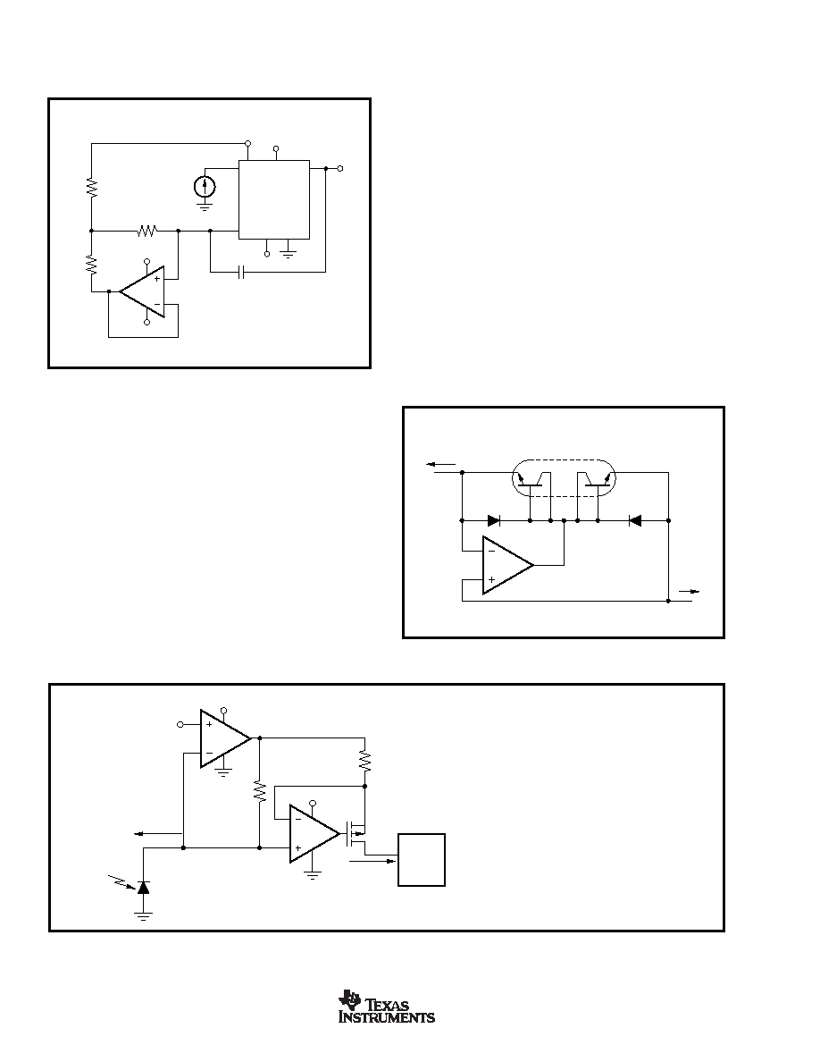
FIGURE 7. Precision Current Inverter/Current Source.
Figure 5 shows a low-level current source using a series
resistor. The low offset op amp reduces the effect of the
LOG112 and LOG2112’s input offset voltage.
FREQUENCY COMPENSATION
Frequency compensation for the LOG112 is obtained by
connecting a capacitor between pins 5 and 14. Frequency
compensation for the LOG2112 is obtained by connecting a
capacitor between pins 2 and 5, or 15 and 12. The size of the
capacitor is a function of the input currents, as shown in the
Typical Characteristic curves (
Minimum Value of Compensa-
tion Capacitor). For any given application, the smallest value
of the capacitor which may be used is determined by the
maximum value of I2 and the minimum value of I1. Larger
values of CC make the LOG112 and LOG2112 more stable,
but reduce the frequency response.
In an application, highest overall bandwidth can be achieved
by detecting the signal level at VOUT, then switching in
appropriate values of compensation capacitors.
NEGATIVE INPUT CURRENTS
The LOG112 and LOG2112 function only with positive input
currents (conventional current flows into input current pins).
In situations where negative input currents are needed, the
circuits in Figures 6, 7, and 8 may be used.
FIGURE 5. Current Source with Offset Compensation.
1M
+2.5mV
100k
–2.5V
+2.5V
OPA335
100
I
1 = 2.5nA to 1mA
I
2 = 2.5nA
V
LOGOUT
C
14
1
910
V–
LOG112
6
5
V+
8
V
REF
Chopper Op Amp
GND
FIGURE 6. Current Inverter/Current Source.
Q
B
National
LM394
I
IN
I
OUT
D
1
OPA703
D
2
Q
A
FREQUENCY RESPONSE
The frequency response curves seen in the Typical Charac-
teristic curves are shown for constant DC I1 and I2 with a
small-signal AC current on one input.
The 3dB frequency response of the LOG112 and LOG2112 are
a function of the magnitude of the input current levels and of the
value of the frequency compensation capacitor. See Typical
Characteristic curve,
3dB Frequency Response for details.
The transient response of the LOG112 and LOG2112 are
different for increasing and decreasing signals. This is due to
the fact that a log amp is a nonlinear gain element and has
different gains at different levels of input signals. Smaller
input currents require greater gain to maintain full dynamic
range, and will slow the frequency response of the LOG112
and LOG2112.
1.5k
Photodiode
10nA to 1mA
+5V
1k
+3.3V(1)
1/2
OPA2335
1/2
OPA2335
BSH203
TLV271 or 1/2 OPA2335
(+3.3V
Back Bias)
LOG112
Pin 1 or Pin 14
NOTE: (1) +3.3V bias is an arbitrary ac level < 5V that also
appears on the
IN through the op amp where it
applies a reverse bias to the photodiode.
相关PDF资料 |
PDF描述 |
|---|---|
| LOG2112AIDWRE4 | LOG OR ANTILOG AMPLIFIER, PDSO16 |
| LOG112AIDE4 | LOG OR ANTILOG AMPLIFIER, PDSO14 |
| LOG112AID | LOG OR ANTILOG AMPLIFIER, 1.4 MHz BAND WIDTH, PDSO14 |
| LOG112AIDRE4 | LOG OR ANTILOG AMPLIFIER, 1.4 MHz BAND WIDTH, PDSO14 |
| LOS4301-2 | 1-OUTPUT 15 W AC-DC REG PWR SUPPLY MODULE |
相关代理商/技术参数 |
参数描述 |
|---|---|
| LOG2112AIDWE4 | 功能描述:对数放大器 Precision Log & Log Ratio Amp RoHS:否 制造商:Texas Instruments 通道数量:3 带宽:3 dB 共模抑制比(最小值): 输入补偿电压:+/- 7 mV 输入电压范围(最大值):5.5 V 工作电源电压:4.5 V to 5.5 V 电源电流:+/- 15 mA 工作温度范围:- 40 C to +85 C 安装风格:SMD/SMT 封装 / 箱体:VQFN-16 封装:Reel |
| LOG2112AIDWR | 功能描述:对数放大器 Precision Log & Log Ratio Amp RoHS:否 制造商:Texas Instruments 通道数量:3 带宽:3 dB 共模抑制比(最小值): 输入补偿电压:+/- 7 mV 输入电压范围(最大值):5.5 V 工作电源电压:4.5 V to 5.5 V 电源电流:+/- 15 mA 工作温度范围:- 40 C to +85 C 安装风格:SMD/SMT 封装 / 箱体:VQFN-16 封装:Reel |
| LOG2112AIDWRE4 | 功能描述:对数放大器 Precision Log & Log Ratio Amp RoHS:否 制造商:Texas Instruments 通道数量:3 带宽:3 dB 共模抑制比(最小值): 输入补偿电压:+/- 7 mV 输入电压范围(最大值):5.5 V 工作电源电压:4.5 V to 5.5 V 电源电流:+/- 15 mA 工作温度范围:- 40 C to +85 C 安装风格:SMD/SMT 封装 / 箱体:VQFN-16 封装:Reel |
| LOGIC | 制造商:SALEAE LLC 功能描述:8 Channel Logic Analyzer |
| LOGIC PCBA | 制造商:Misc 功能描述: |
发布紧急采购,3分钟左右您将得到回复。