- 您现在的位置:买卖IC网 > PDF目录44716 > LOG2112AIDW (TEXAS INSTRUMENTS INC) LOG OR ANTILOG AMPLIFIER, 1.4 MHz BAND WIDTH, PDSO16 PDF资料下载
参数资料
| 型号: | LOG2112AIDW |
| 厂商: | TEXAS INSTRUMENTS INC |
| 元件分类: | 模拟运算功能 |
| 英文描述: | LOG OR ANTILOG AMPLIFIER, 1.4 MHz BAND WIDTH, PDSO16 |
| 封装: | ROHS COMPLIANT, PLASTIC, MS-013AA, SOIC-16 |
| 文件页数: | 3/20页 |
| 文件大小: | 621K |
| 代理商: | LOG2112AIDW |
LOG112, 2112
11
SBOS246D
www.ti.com
also
VV
RR
R
OUT
L
=
+
12
1
(9)
V
RR
R
nV
I
OUT
T
=
+
12
1
2
log
(10)
or
V
V LOG
I
OUT =
(.
)
05
1
2
(11)
Using the base-emitter voltage relationship of matched
bipolar transistors, the LOG112 establishes a logarith-
mic function of input current ratios. Beginning with the
base-emitter voltage defined as:
VV
I
where V
kT
q
BE
T
C
S
T
==
ln
:
(1)
k = Boltzmann’s constant = 1.381 10–23
T = Absolute temperature in degrees Kelvin
q = Electron charge = 1.602 10–19 Coulombs
IC = Collector current
IS = Reverse saturation current
From the circuit in Figure 12:
VV
V
LBE
BE
=
12
–
(2)
Substituting (1) into (2) yields:
VV
I
V
I
LT
S
T
S
=
1
2
ln
–
ln
(3)
If the transistors are matched and isothermal and
VTI = VT2, then (3) becomes:
VV
I
LT
SS
=
1
12
ln
– ln
(4)
VV
I
and
ce
LT
=
ln
sin
1
2
(5)
ln
. log
xx
= 23
10
(6)
Vn V
I
LT
=
log 1
2
(7)
where n = 2.3
(8)
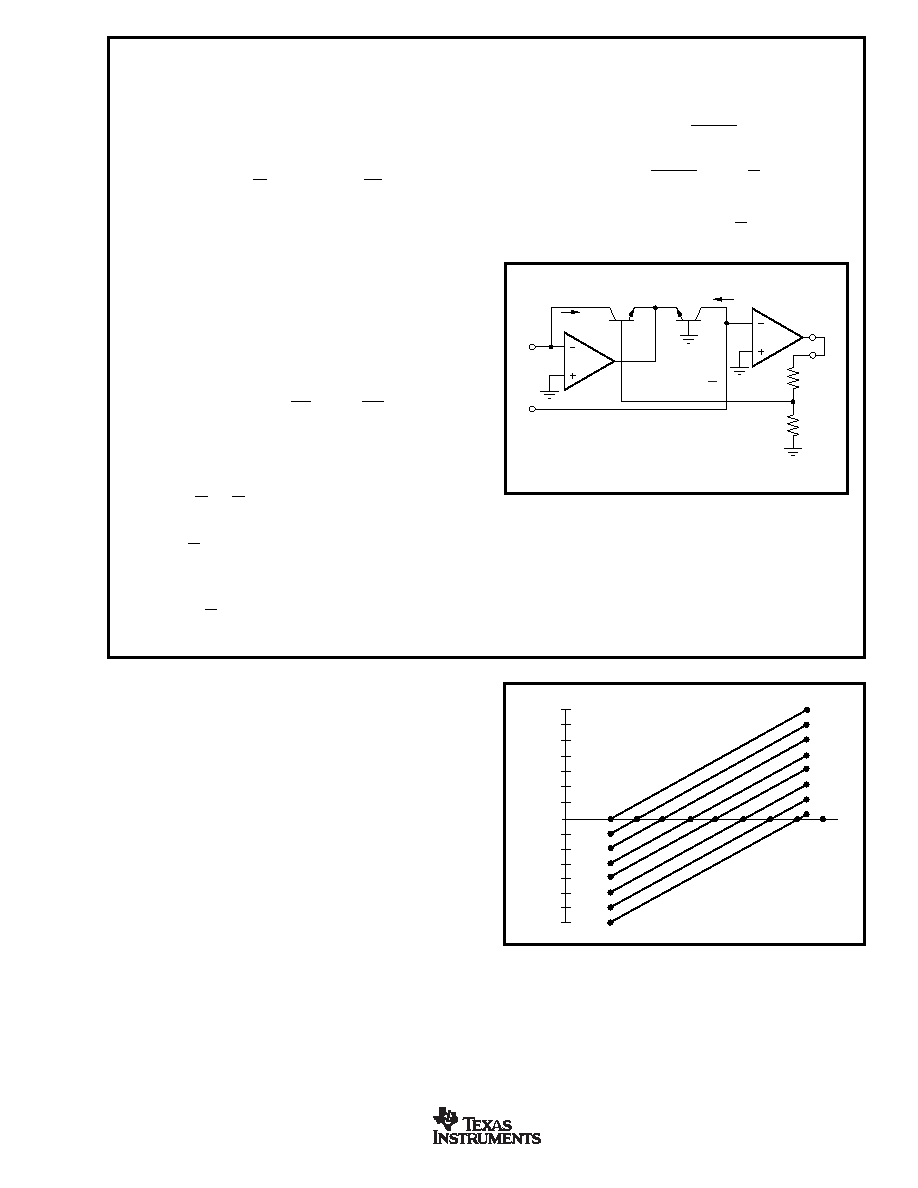
INSIDE THE LOG112
FIGURE 13. Simplified Model of a Log Amplifier.
A
2
A
1
I
1
Q
1
Q
2
I
2
I
1
I
2
++
––
R
2
V
OUT
V
L
R
1
V
BE1
V
BE2
V
OUT = (0.5V)LOG
I
1
I
2
NOTE: R1 is a metal resistor used to compensate for gain
over temperature.
DEFINITION OF TERMS
TRANSFER FUNCTION
The ideal transfer function is:
VLOGOUT = (0.5V)LOG (I1/I2)
Figure 14 shows the graphical representation of the transfer
over valid operating range for the LOG112 and LOG2112.
ACCURACY
Accuracy considerations for a log ratio amplifier are some-
what more complicated than for other amplifiers. This is
because the transfer function is nonlinear and has two
inputs, each of which can vary over a wide dynamic range.
The accuracy for any combination of inputs is determined
from the total error specification.
TOTAL ERROR
The total error is the deviation (expressed in mV) of the actual
output from the ideal output of VLOGOUT = (0.5V)LOG (I1/I2).
Thus,
VLOGOUT(ACTUAL) = VLOGOUT(IDEAL) ± Total Error
(6)
It represents the sum of all the individual components of error
normally associated with the log amp when operated in the
current input mode. The worst-case error for any given ratio
of I1/I2 is the largest of the two errors when I1 and I2 are
considered separately. Temperature can affect total error.
FIGURE 14. Transfer Function with Varying I2 and I1.
3.0
3.5
2.0
2.5
1.0
1.5
0.5
0
–3.0
–3.5
–2.0
–2.5
–1.0
–0.5
–1.5
1nA
10nA
100nA 1
A
10
A
100
A
1mA
10m
A
100pA
V
OUT
(V)
I 2 =
100pA
I 2 =
1nA
I 2 =
10nA
I 2 =
100nA
I 2 =
1
A
I 2 =
10
A
I 2 =
100
A
I 2 =
1m
A
I
1
V
LOGOUT = (0.5V)LOG (I1/I2)
相关PDF资料 |
PDF描述 |
|---|---|
| LOG2112AIDWRE4 | LOG OR ANTILOG AMPLIFIER, PDSO16 |
| LOG112AIDE4 | LOG OR ANTILOG AMPLIFIER, PDSO14 |
| LOG112AID | LOG OR ANTILOG AMPLIFIER, 1.4 MHz BAND WIDTH, PDSO14 |
| LOG112AIDRE4 | LOG OR ANTILOG AMPLIFIER, 1.4 MHz BAND WIDTH, PDSO14 |
| LOS4301-2 | 1-OUTPUT 15 W AC-DC REG PWR SUPPLY MODULE |
相关代理商/技术参数 |
参数描述 |
|---|---|
| LOG2112AIDWE4 | 功能描述:对数放大器 Precision Log & Log Ratio Amp RoHS:否 制造商:Texas Instruments 通道数量:3 带宽:3 dB 共模抑制比(最小值): 输入补偿电压:+/- 7 mV 输入电压范围(最大值):5.5 V 工作电源电压:4.5 V to 5.5 V 电源电流:+/- 15 mA 工作温度范围:- 40 C to +85 C 安装风格:SMD/SMT 封装 / 箱体:VQFN-16 封装:Reel |
| LOG2112AIDWR | 功能描述:对数放大器 Precision Log & Log Ratio Amp RoHS:否 制造商:Texas Instruments 通道数量:3 带宽:3 dB 共模抑制比(最小值): 输入补偿电压:+/- 7 mV 输入电压范围(最大值):5.5 V 工作电源电压:4.5 V to 5.5 V 电源电流:+/- 15 mA 工作温度范围:- 40 C to +85 C 安装风格:SMD/SMT 封装 / 箱体:VQFN-16 封装:Reel |
| LOG2112AIDWRE4 | 功能描述:对数放大器 Precision Log & Log Ratio Amp RoHS:否 制造商:Texas Instruments 通道数量:3 带宽:3 dB 共模抑制比(最小值): 输入补偿电压:+/- 7 mV 输入电压范围(最大值):5.5 V 工作电源电压:4.5 V to 5.5 V 电源电流:+/- 15 mA 工作温度范围:- 40 C to +85 C 安装风格:SMD/SMT 封装 / 箱体:VQFN-16 封装:Reel |
| LOGIC | 制造商:SALEAE LLC 功能描述:8 Channel Logic Analyzer |
| LOGIC PCBA | 制造商:Misc 功能描述: |
发布紧急采购,3分钟左右您将得到回复。