- 您现在的位置:买卖IC网 > PDF目录20808 > LP5521YQX/NOPB (National Semiconductor)IC LED DRIVER RGB 24-LLP PDF资料下载
参数资料
| 型号: | LP5521YQX/NOPB |
| 厂商: | National Semiconductor |
| 文件页数: | 13/44页 |
| 文件大小: | 0K |
| 描述: | IC LED DRIVER RGB 24-LLP |
| 标准包装: | 4,500 |
| 系列: | PowerWise® |
| 恒定电流: | 是 |
| 拓扑: | PWM,切换式电容器(充电泵) |
| 输出数: | 3 |
| 内部驱动器: | 是 |
| 类型 - 主要: | 背光,照明管理装置(LMU) |
| 类型 - 次要: | RGB |
| 频率: | 1.25MHz |
| 电源电压: | 2.7 V ~ 5.5 V |
| 输出电压: | 4.55V |
| 安装类型: | 表面贴装 |
| 封装/外壳: | 24-WFQFN 裸露焊盘 |
| 供应商设备封装: | 24-LLP |
| 包装: | 带卷 (TR) |
| 工作温度: | -30°C ~ 85°C |
| 其它名称: | LP5521YQX |
第1页第2页第3页第4页第5页第6页第7页第8页第9页第10页第11页第12页当前第13页第14页第15页第16页第17页第18页第19页第20页第21页第22页第23页第24页第25页第26页第27页第28页第29页第30页第31页第32页第33页第34页第35页第36页第37页第38页第39页第40页第41页第42页第43页第44页
�� ����
����
����SNVS441F� –� JANUARY� 2007� –� REVISED� FEBRUAY� 2013�
�FUNCTIONAL� DESCRIPTION�
�CHARGE� PUMP� OPERATIONAL� DESCRIPTION�
�OVERVIEW�
�The� LP5521� includes� a� pre-regulated� switched-capacitor� charge� pump� with� a� programmable� voltage�
�multiplication� of� 1� and� 1.5x.�
�On� 1.5x� mode� by� combining� the� principles� of� a� switched-capacitor� charge� pump� and� a� linear� regulator,� it�
�generates� a� regulated� 4.5V� output� from� Li-Ion� input� voltage� range.� A� two-phase� non-overlapping� clock� generated�
�internally� controls� the� operation� of� the� charge� pump.� During� the� charge� phase,� both� flying� capacitors� (C� FLY1� and�
�C� FLY2� )� are� charged� from� input� voltage.� In� the� pump� phase� that� follows,� the� flying� capacitors� are� discharged� to�
�output.� A� traditional� switched� capacitor� charge� pump� operating� in� this� manner� will� use� switches� with� very� low� on-�
�resistance,� ideally� 0� ?� ,� to� generate� an� output� voltage� that� is� 1.5x� the� input� voltage.� The� LP5521� regulates� the�
�output� voltage� by� controlling� the� resistance� of� the� input-connected� pass-transistor� switches� in� the� charge� pump.�
�OUTPUT� RESISTANCE�
�At� lower� input� voltages,� the� charge� pump� output� voltage� may� degrade� due� to� effective� output� resistance� (R� OUT� )� of�
�the� charge� pump.� The� expected� voltage� drop� can� be� calculated� by� using� a� simple� model� for� the� charge� pump�
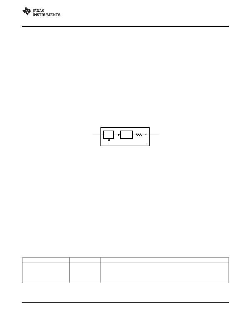
�illustrated� in� following� figure.�
�Charge� Pump�
�V� IN�
�REG�
�9?�
�1.5� x�
�1.5� [� 9?�
�V� OUT�
�R� OUT�
�Figure� 23.�
�The� model� shows� a� linear� pre-regulation� block� (REG),� a� voltage� multiplier� (1.5x),� and� an� output� resistance�
�(R� OUT� ).� Output� resistance� models� the� output� voltage� drop� that� is� inherent� to� switched� capacitor� converters.� The�
�output� resistance� is� 3.5� ?� (typ),� and� is� function� of� switching� frequency,� input� voltage,� flying� capacitors’�
�capacitance� value,� internal� resistances� of� switches� and� ESR� of� flying� capacitors.� When� the� output� voltage� is� in�
�regulation,� the� regulator� in� the� model� controls� the� voltage� V’� to� keep� the� output� voltage� equal� to� 4.5V� (typ).� With�
�increased� output� current,� the� voltage� drop� across� R� OUT� increases.� To� prevent� drop� in� output� voltage,� the� voltage�
�drop� across� the� regulator� is� reduced,� V’� increases,� and� V� OUT� remains� at� 4.5V.� When� the� output� current� increases�
�to� the� point� that� there� is� zero� voltage� drop� across� the� regulator,� V’� equals� the� input� voltage,� and� the� output�
�voltage� is� “on� the� edge”� of� regulation.� Additional� output� current� causes� the� output� voltage� to� fall� out� of� regulation,�
�so� that� the� operation� is� similar� to� a� basic� open-loop� 1.5x� charge� pump.� In� this� mode,� output� current� results� in�
�output� voltage� drop� proportional� to� the� output� resistance� of� the� charge� pump.� The� out-of-regulation� output�
�voltage� can� be� approximated� by:� V� OUT� =� 1.5� x� V� IN� –� I� OUT� x� R� OUT� .�
�CONTROLLING� CHARGE� PUMP�
�Charge� pump� is� controlled� with� two� CP_MODE� bits� in� register� 08H.� When� both� bits� are� low,� charge� pump� is�
�disabled� and� output� voltage� is� pulled� down� with� 300� k� ?� .� Charge� pump� can� be� forced� to� bypass� mode,� so� battery�
�voltage� is� going� directly� to� RGB� outputs.� In� 1.5x� mode� output� voltage� is� boosted� to� 4.5V.� In� automatic� mode,�
�charge� pump� operation� mode� is� defined� by� LED� outputs� saturation� like� described� in� LED� Forward� Voltage�
�Monitoring.� In� following� table� are� listed� operation� modes� and� selection� bits.�
�Table� 1.� CONFIG� register� (08H):�
�Name�
�CP_MODE�
�Bit�
�4:3�
�Description�
�Charge� Pump� Operation� Mode�
�00b� =� OFF�
�01b� =� Forced� to� bypass� mode� (1x)�
�10b� =� Forced� to� 1.5x� mode�
�11b� =� Automatic� mode� selection�
�Copyright� ?� 2007–2013,� Texas� Instruments� Incorporated�
�Product� Folder� Links:� LP5521�
��13�
�相关PDF资料 |
PDF描述 |
|---|---|
| REC7.5-2412DRW/H2/A/M/SMD | CONV DC/DC 7.5W 18-36VIN +/-12V |
| NPS 2-T126 0.360 OHM 1% | RES .36 OHM 25W 1% DPAK |
| CAT4008V-T1 | IC LED DRIVER LINEAR 16-SOIC |
| P51-15-S-UB-D-4.5OVP-000-000 | SENSOR 15PSI 1/8-27NPT .5-4.5V |
| REC3-1205SRW/H6/A/M | CONV DC/DC 3W 9-18VIN 05VOUT |
相关代理商/技术参数 |
参数描述 |
|---|---|
| LP5522 | 制造商:NSC 制造商全称:National Semiconductor 功能描述:Programmable LED Driver |
| LP5522TM | 制造商:Texas Instruments 功能描述:LED DRVR 1Segment 3.3V/5V 6-Pin uSMD T/R |
| LP5522TM/NOPB | 功能描述:LED照明驱动器 RoHS:否 制造商:STMicroelectronics 输入电压:11.5 V to 23 V 工作频率: 最大电源电流:1.7 mA 输出电流: 最大工作温度: 安装风格:SMD/SMT 封装 / 箱体:SO-16N |
| LP5522TMEV | 功能描述:电源管理IC开发工具 LP5522TMEV EVAL BOARD RoHS:否 制造商:Maxim Integrated 产品:Evaluation Kits 类型:Battery Management 工具用于评估:MAX17710GB 输入电压: 输出电压:1.8 V |
| LP5522TMX | 制造商:NSC 制造商全称:National Semiconductor 功能描述:Programmable LED Driver |
发布紧急采购,3分钟左右您将得到回复。