- 您现在的位置:买卖IC网 > PDF目录19400 > LSM2-T/6-W3-C (Murata Power Solutions Inc)CONV DC/DC 19.8W 6A 5V SMD PDF资料下载
参数资料
| 型号: | LSM2-T/6-W3-C |
| 厂商: | Murata Power Solutions Inc |
| 文件页数: | 15/17页 |
| 文件大小: | 0K |
| 描述: | CONV DC/DC 19.8W 6A 5V SMD |
| 标准包装: | 1 |
| 系列: | LSM2 |
| 类型: | 非隔离(POL) |
| 输出数: | 1 |
| 电压 - 输入(最小): | 2.4V |
| 电压 - 输入(最大): | 5.5V |
| Voltage - Output 1: | 0.75 ~ 3.3 V |
| 电流 - 输出(最大): | 6A |
| 电源(瓦) - 制造商系列: | 19W |
| 安装类型: | 表面贴装 |
| 封装/外壳: | 8-DIP SMD 模块 |
| 尺寸/尺寸: | 1.30" L x 0.53" W x 0.34" H(33.0mm x 13.5mm x 8.6mm) |
| 包装: | 标准包装 |
| 工作温度: | -40°C ~ 85°C |
| 效率: | 95.5% |
| 电源(瓦特)- 最大: | 19.8W |
| 产品目录页面: | 2719 (CN2011-ZH PDF) |
| 其它名称: | 811-1781-6 |
�� �
�
�LSM2� Series�
�Single� Output,� Non-Isolated�
�Selectable-Output� POL� DC/DC� Converters�
�Guidelines� for� Sequence/Track� Applications�
�[1]� Leave� the� converter’s� On/Off� Enable� control� (if� installed)� in� the� On� setting.�
�Normally,� you� should� just� leave� the� On/Off� pin� open.�
�[2]� Allow� the� converter� to� stabilize� (typically� less� than� 20� mS� after� +V� IN� power�
�on)� before� raising� the� Sequence� input.� Also,� if� you� wish� to� have� a� ramped�
�power� down,� leave� +V� IN� powered� all� during� the� down� ramp.� Do� not� simply�
�shut� off� power.�
�[3]� If� you� do� not� use� the� Sequence/Track� pin,� leave� it� open� or� tied� to� +V� IN� .�
�[4]� Observe� the� Output� slew� rate� relative� to� the� Sequence� input.� A� rough�
�guide� is� 2� Volts� per� millisecond� maximum� slew� rate.� If� you� exceed� this�
�slew� rate� on� the� Sequence� pin,� the� converter� will� simply� ramp� up� at�
�it’s� maximum� output� slew� rate� (and� will� not� necessarily� track� the� faster�
�Sequence� input).� The� reason� to� carefully� consider� the� slew� rate� limitation�
�is� in� case� you� want� two� different� POL’s� to� precisely� track� each� other.�
�[5]� Be� aware� of� the� input� characteristics� of� the� Sequence� pin.� The� high� input�
�impedance� affects� the� time� constant� of� any� small� external� ramp� capacitor.�
�And� the� bias� current� will� slowly� charge� up� any� external� caps� over� time�
�if� they� are� not� grounded.� The� internal� pull-up� resistor� to� +V� IN� is� typically�
�[8]� If� one� converter� is� slaving� to� another� master� converter,� there� will� be� a� very�
�short� phase� lag� between� the� two� converters.� This� can� usually� be� ignored.�
�[9]� You� may� connect� two� or� more� Sequence� inputs� in� parallel� from� two� con-�
�verters.� Be� aware� of� the� increasing� pull-up� bias� current� and� reduced� input�
�impedance.�
�[10]� Any� external� capacitance� added� to� the� converter’s� output� may� affect� ramp�
�up/down� times� and� ramp� tracking� accuracy.�
�Power� Good� Output�
�The� Power� Good� Output� consists� of� an� unterminated� BSS138� small� signal�
�?eld� effect� transistor� and� a� dual� window� comparator� input� circuit� driving� the�
�gate� of� the� FET.� Power� Good� is� TRUE� (open� drain,� high� impedance� state)� if� the�
�converter’s� power� output� voltage� is� within� about� ±10%� of� the� setpoint.� Thus,�
�the� PG� TRUE� condition� indicates� that� the� converter� is� approximately� within�
�regulation.� Since� an� overcurrent� condition� occurs� at� about� 2%� output� voltage�
�reduction,� the� Power� Good� does� not� directly� measure� an� output� overcurrent�
�condition� at� rated� maximum� output� current.� However,� gross� overcurrent� or� an�
�output� short� circuit� will� set� Power� Good� to� FALSE� (+0.2V� saturation,� low� imped-�
�ance� condition).�
�400k� ?� to� 1M� ?� .�
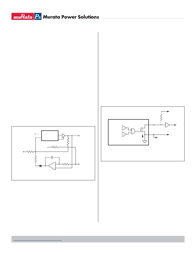
�Notice� in� the� simpli?ed� Sequence/Track� equivalent� circuit� (Figure� 17)� that�
�a� blocking� diode� effectively� disconnects� this� circuit� when� the� Sequence/�
�Track� pin� is� pulled� up� to� +V� IN� or� left� open.�
�Figure� 18.� Equivalent� Power� Good� Circuit�
�Using� a� simple� connection� to� external� logic� (and� returned� to� the� converter’s�
�Common� connection),� the� Power� Good� output� is� unterminated� so� that� the� user�
�Figure� 17.� Sequence/Track� Simpli?ed� Equivalent� Schematic�
�[6]� Allow� the� converter� to� eventually� achieve� its� full-rated� setpoint� output�
�voltage.� Do� not� remain� in� ramp� up/down� mode� inde?nitely.� The� converter�
�is� characterized� and� meets� all� its� speci?cations� only� at� the� setpoint� volt-�
�age� (plus� or� minus� any� trim� voltage).� During� the� ramp-up� phase,� the� con-�
�verter� is� not� considered� fully� in� regulation.� This� may� affect� performance�
�may� adapt� the� output� to� a� variety� of� logic� families.� The� PG� pin� may� therefore�
�be� used� with� logic� voltages� which� are� not� necessarily� the� same� as� the� input�
�or� output� power� voltages.� Install� an� external� pullup� resistor� to� the� logic� supply�
�voltage� which� is� compatible� with� your� logic� system.� When� the� Power� Good� is�
�out� of� limit,� the� FET� is� at� saturation,� approximately� +0.2V� output.� Keep� this�
�LOW� (FALSE)� pulldown� current� to� less� than� 10mA.�
�Please� note� that� Power� Good� is� brie?y� false� during� Sequence� ramp-up.�
�Ignore� Power� Good� while� in� transition.�
�with� excessive� high� current� loads� at� turn-on.�
�[7]� The� Sequence� is� a� sensitive� input� into� the� feedback� control� loop� of� the�
�converter.� Avoid� noise� and� long� leads� on� this� input.� Keep� all� wiring� very�
�short.� Use� shielding� if� necessary.� Consider� adding� a� small� parallel� ceramic�
�capacitor� across� the� Sequence/Track� input� (see� Figure� 16)� to� block� any�
�external� high� frequency� noise.�
�www.murata-ps.com/support�
�M� D� C_LSM2� Series.C01� Δ� Page� 15� of� 17�
�相关PDF资料 |
PDF描述 |
|---|---|
| MAX7503MUA+T | IC TEMP SENSOR DIGIT 8-UMAX |
| VI-22Y-CY-F2 | CONVERTER MOD DC/DC 3.3V 33W |
| VI-22Y-CX-F4 | CONVERTER MOD DC/DC 3.3V 49.5W |
| RSO-4809SZ | CONV DC/DC 1W 18-72VIN 09VOUT |
| RSO-4805SZ | CONV DC/DC 1W 18-72VIN 05VOUT |
相关代理商/技术参数 |
参数描述 |
|---|---|
| LSM2U | 功能描述:限位开关 LIMIT SWITCH RoHS:否 制造商:Honeywell 触点形式:SPDT 执行器:Non-Contact 电流额定值:30 mA 电压额定值 AC: 电压额定值 DC:3.6 V 工作力:10 g IP 等级:IP 67 NEMA 额定值:1, 4, 12, 13 端接类型:4-Pin M12 Connector 安装:SMD/SMT |
| LSM-3.3/10-D12 | 功能描述:DC/DC转换器 33W 12V to 3.3V 10A SMT Package RoHS:否 制造商:Murata 产品: 输出功率: 输入电压范围:3.6 V to 5.5 V 输入电压(标称): 输出端数量:1 输出电压(通道 1):3.3 V 输出电流(通道 1):600 mA 输出电压(通道 2): 输出电流(通道 2): 安装风格:SMD/SMT 封装 / 箱体尺寸: |
| LSM-3.3/10-D12-C | 功能描述:DC/DC转换器 33W 12V to 3.3V 10A RoHS:否 制造商:Murata 产品: 输出功率: 输入电压范围:3.6 V to 5.5 V 输入电压(标称): 输出端数量:1 输出电压(通道 1):3.3 V 输出电流(通道 1):600 mA 输出电压(通道 2): 输出电流(通道 2): 安装风格:SMD/SMT 封装 / 箱体尺寸: |
| LSM-3.3/10-D12EB | 制造商:MURATA 制造商全称:Murata Manufacturing Co., Ltd. 功能描述:10 Amp DC/DC Power Converter Evaluation Boards |
| LSM-3.3/10-D5 | 功能描述:DC/DC转换器 33W 5V to 3.3V 10A SMT Package RoHS:否 制造商:Murata 产品: 输出功率: 输入电压范围:3.6 V to 5.5 V 输入电压(标称): 输出端数量:1 输出电压(通道 1):3.3 V 输出电流(通道 1):600 mA 输出电压(通道 2): 输出电流(通道 2): 安装风格:SMD/SMT 封装 / 箱体尺寸: |
发布紧急采购,3分钟左右您将得到回复。