- 您现在的位置:买卖IC网 > PDF目录32308 > LSP3171MSAD (LITE-ON SEMICONDUCTOR CORP) SWITCHING REGULATOR, 470 kHz SWITCHING FREQ-MAX, PDSO10 PDF资料下载
参数资料
| 型号: | LSP3171MSAD |
| 厂商: | LITE-ON SEMICONDUCTOR CORP |
| 元件分类: | 稳压器 |
| 英文描述: | SWITCHING REGULATOR, 470 kHz SWITCHING FREQ-MAX, PDSO10 |
| 封装: | MSOP-10 |
| 文件页数: | 2/9页 |
| 文件大小: | 330K |
| 代理商: | LSP3171MSAD |
Liteon Semiconductor Corporation
LSP3171
MSOP10L 2A Step Down DC/DC Converter
Rev1.4
2/9
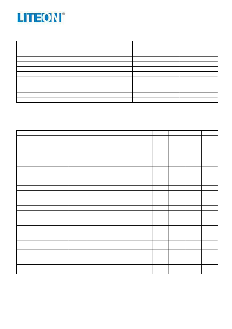
ABSOLUTE MAXIMUM RATINGS
Parameter
Value
Unit
IN Supply Voltage
-0.3 to 20
V
SW Voltage
-1 to VIN + 1
V
BS Voltage
VSW – 0.3 to VSW + 8
V
EN, FB, COMP Voltage
-0.3 to 7
V
Continuous SW Current
Internally limited
A
Junction to Ambient Thermal Resistance (θJA)
80
°C/W
Junction to CaseThermal Resistance (θJC)
20
°C/W
Maximum Power Dissipation
1.6
W
Operating Junction Temperature
-40 to 150
°C
Storage Temperature
-55 to 150
°C
Lead Temperature (Soldering, 10 sec)
300
°C
(Note: Exceeding these limits may damage the device. Exposure to absolute maximum rating conditions for long
periods may affect device reliability.)
ELECTRICAL CHARACTERISTICS
(VIN = 12V, TA= 25°C unless otherwise specified.)
Parameter
Symbol
Test Conditions
Min.
Typ.
Max.
Unit
Input Voltage
VIN
VOUT = 5V, ILOAD = 0A to 1A
7
18
V
Feedback Voltage
VFB
7V ≤ VIN ≤ 20V, VCOMP = 1.5V
1.185
1.222
1.258
V
Saturation voltage of output
driver
VCEsat
VIN=12V ILOAD=1A
500
mV
SW Leakage
VEN = 0
0
10
A
Current Limit
ILIMT
2.6
A
COMP to Current Limit
Transconductance
GCOMP
2.5
A/V
Error Amplifier
Transconductance
GEA
ICOMP = ±10A
850
A/V
Error Amplifier DC Gain
AVEA
350
V/V
Switching Frequency
fSW
350
400
470
KHz
Short Circuit Switching
Frequency
VFB = 0
50
KHz
Maximum Duty Cycle
DMAX
VFB = 1.1V
90
95
%
Minimum Duty Cycle
VFB = 1.4V
0
%
V COMP Pin Maximum
Switching Threshold
Duty cycle = 0%
0.35
V
Minimum Boost Voltage
Above Switch
I SW = 2A
1.8
2.7
V
Enable Threshold Voltage
Hysteresis = 0.1V
2.0
2.5
V
Enable Pull Up Current
Pin pulled up to 4.5V typically when
left unconnected
2
A
Supply Current in Shutdown
VEN = 0
8
40
A
IC Supply Current in
Operation
VEN = 3V, VFB = 1.4V
2.2
mA
Thermal Shutdown
Temperature
Hysteresis = 10°C
160
°C
相关PDF资料 |
PDF描述 |
|---|---|
| LT1009CPWG4 | 1-OUTPUT TWO TERM VOLTAGE REFERENCE, 2.5 V, PDSO8 |
| LT1009IPWG4 | 1-OUTPUT TWO TERM VOLTAGE REFERENCE, 2.5 V, PDSO8 |
| LT140SAB | SPECIALTY ANALOG CIRCUIT, PDSO4 |
| LT230A | SPECIALTY ANALOG CIRCUIT, PDSO4 |
| LT3483AEDC#TRMPBF | 0.46 A SWITCHING REGULATOR, PDSO8 |
相关代理商/技术参数 |
参数描述 |
|---|---|
| LSP32-K2-RGBA | 制造商:Dialight 功能描述:LED MODULE 32X K2 RGBA |
| LSP-32K2-RGBW | 制造商:Dialight 功能描述: |
| LSP32-K2-RGBW | 制造商:Dialight 功能描述:LED MODULE 32X K2 RGBW |
| LSP-32K2-WWWW | 制造商:Dialight 功能描述: |
| LSP32-K2-WWWW | 制造商:Dialight 功能描述:LED MODULE 32X K2 WWWW |
发布紧急采购,3分钟左右您将得到回复。