- 您现在的位置:买卖IC网 > PDF目录14064 > LT1108CS8-5#TR (Linear Technology)IC REG BUCK BST INV 5V .4A 8SOIC PDF资料下载
参数资料
| 型号: | LT1108CS8-5#TR |
| 厂商: | Linear Technology |
| 文件页数: | 9/12页 |
| 文件大小: | 0K |
| 描述: | IC REG BUCK BST INV 5V .4A 8SOIC |
| 标准包装: | 2,500 |
| 类型: | 降压(降压),升压(升压),反相 |
| 输出类型: | 固定 |
| 输出数: | 1 |
| 输出电压: | 5V |
| 输入电压: | 2 V ~ 30 V |
| 频率 - 开关: | 19kHz |
| 电流 - 输出: | 400mA |
| 同步整流器: | 无 |
| 工作温度: | 0°C ~ 70°C |
| 安装类型: | 表面贴装 |
| 封装/外壳: | 8-SOIC(0.154",3.90mm 宽) |
| 包装: | 带卷 (TR) |
| 供应商设备封装: | 8-SOIC |
�� �
�
�LT1108�
�A� PPLICATI�
�S� I� FOR� ATIO�
�I� PEAK� =�
�V� IN� ?� V� SW� ?� V� OUT�
�L�
�t� ON�
�(� 22� )�
�HIGHER� CURRENT� STEP-DOWN� OPERATION�
�Output� current� can� be� increased� by� using� a� discrete� PNP�
�When� the� switch� turns� off,� the� SW2� pin� falls� rapidly� and�
�actually� goes� below� ground.� D1� turns� on� when� SW2�
�reaches� 0.4V� below� ground.� D1� MUST� BE� A� SCHOTTKY�
�DIODE.� The� voltage� at� SW2� must� never� be� allowed� to� go�
�below� –0.5V.� A� silicon� diode� such� as� the� 1N4933� will� allow�
�SW2� to� go� to� –0.8V,� causing� potentially� destructive� power�
�dissipation� inside� the� LT1108.� Output� voltage� is� deter-�
�pass� transistor� as� shown� in� Figure� 3.� R1� serves� as� a�
�current� limit� sense.� When� the� voltage� drop� across� R1�
�equals� 0.5V� BE� ,� the� switch� turns� off.� As� shown,� switch�
�current� is� limited� to� 2A.� Inductor� value� can� be� calculated�
�based� on� formulas� in� the� Inductor� Selection� Step-Down�
�Converter� section� with� the� following� conservative� expres-�
�sion� for� V� SW� :�
�mined� by�
�V� SW� =� V� R� 1� +� V� Q� 1� SAT� ≈� 1� .� 0� V�
�(� 24� )�
�V� OUT� =� ?� 1� +�
�(�
�R� 1� ?�
�?�
�?�
�R� 2� ?�
�?� 1� .� 245� V�
�)�
�(� 23� )�
�R2� provides� a� current� path� to� turn� off� Q1.� R3� provides� base�
�drive� to� Q1.� R4� and� R5� set� output� voltage.� A� PMOS� FET� can�
�be� used� in� place� of� Q1� when� V� IN� is� between� 10V� and� 20V.�
�R3� programs� switch� current� limit.� This� is� especially� impor-�
�tant� in� applications� where� the� input� varies� over� a� wide�
�range.� Without� R3,� the� switch� stays� on� for� a� fixed� time� each�
�cycle.� Under� certain� conditions� the� current� in� L1� can� build�
�V� IN�
�30V�
�MAX�
�R1�
�0.15� ?�
�Q1�
�ZETEX� ZTX749�
�R2�
�100� ?�
�L1�
�V� OUT�
�+�
�(� )�
�V� OUT� =� 1.245V� 1� +� R5�
�up� to� excessive� levels,� exceeding� the� switch� rating� and/or�
�saturating� the� inductor.� The� 100� ?� resistor� programs� the�
�switch� to� turn� off� when� the� current� reaches� approximately�
�700mA.� When� using� the� LT1108� in� step-down� mode,�
�output� voltage� should� be� limited� to� 6.2V� or� less.� Higher�
�output� voltages� can� be� accommodated� by� inserting� a�
�1N5818� diode� in� series� with� the� SW2� pin� (anode� connected�
�to� SW2).�
�+�
�C2�
�V� IN� I� L�
�SW1�
�LT1108�
�FB�
�GND� SW2�
�R6�
�100� ?�
�R3�
�330� ?�
�R4�
�R5�
�D1�
�1N5821�
�C1�
�R4�
�LT1108� ?� F03�
�V� IN�
�R3�
�100� ?�
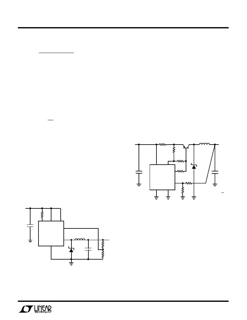
�Figure� 3.� Q1� Permits� Higher� Current� Switching�
�The� LT1108� Functions� as� Controller�
�+�
�C2�
�I� LIM�
�V� IN�
�LT1108�
�SW1�
�FB�
�SW2�
�L1�
�V� OUT�
�INVERTING� CONFIGURATIONS�
�The� LT1108� can� be� configured� as� a� positive-to-negative�
�converter� (Figure� 4),� or� a� negative-to-positive� converter�
�GND�
�D1�
�1N5818�
�+�
�C1�
�R2�
�R1�
�(Figure� 5).� In� Figure� 4,� the� arrangement� is� very� similar� to� a�
�step-down,� except� that� the� high� side� of� the� feedback� is�
�referred� to� ground.� This� level� shifts� the� output� negative.� As�
�Figure� 2.� Step-Down� Mode� Hookup�
�LT1108� ?� F02�
�in� the� step-down� mode,� D1� must� be� a� Schottky� diode,�
�and� ?� V� OUT� ?� should� be� less� than� 6.2V.� More� negative� output�
�voltages� can� be� accommodated� as� in� the� prior� section.�
�In� Figure� 5,� the� input� is� negative� while� the� output� is� positive.�
�In� this� configuration,� the� magnitude� of� the� input� voltage� can�
�be� higher� or� lower� than� the� output� voltage.� A� level� shift,�
�9�
�相关PDF资料 |
PDF描述 |
|---|---|
| RBM10DTAN-S664 | CONN EDGECARD 20POS R/A .156 SLD |
| 50MS70.33MEFCTZ4X7 | CAP ALUM 0.33UF 50V 20% RADIAL |
| RBM10DTAD-S664 | CONN EDGECARD 20POS R/A .156 SLD |
| EBM22DTAN-S664 | CONN EDGECARD 44POS R/A .156 SLD |
| VE-JV1-CZ-F1 | CONVERTER MOD DC/DC 12V 25W |
相关代理商/技术参数 |
参数描述 |
|---|---|
| LT1108CS8PBF | 制造商:Linear Technology 功能描述:DC/DC Converter Adj Micropower 2-30V SO8 |
| LT1109 | 制造商:LINER 制造商全称:Linear Technology 功能描述:Micropower Low Cost DC/DC Converter Adjustable and Fixed 5V, 12V |
| LT1109-12 | 制造商:LINER 制造商全称:Linear Technology 功能描述:Micropower Low Cost DC/DC Converter Adjustable and Fixed 5V, 12V |
| LT1109-5 | 制造商:LINER 制造商全称:Linear Technology 功能描述:Micropower Low Cost DC/DC Converter Adjustable and Fixed 5V, 12V |
| LT1109A | 制造商:LINER 制造商全称:Linear Technology 功能描述:Micropower DC/DC Converter Flash Memory VPP Generator Adjustable and Fixed 5V, 12V |
发布紧急采购,3分钟左右您将得到回复。