- 您现在的位置:买卖IC网 > PDF目录1821 > LT1129MPST-3.3#TRPBF (Linear Technology)IC REG LDO 3.3V .7A SOT223 PDF资料下载
参数资料
| 型号: | LT1129MPST-3.3#TRPBF |
| 厂商: | Linear Technology |
| 文件页数: | 10/16页 |
| 文件大小: | 0K |
| 描述: | IC REG LDO 3.3V .7A SOT223 |
| 产品培训模块: | More Information on LDOs |
| 标准包装: | 2,000 |
| 稳压器拓扑结构: | 正,固定式 |
| 输出电压: | 3.3V |
| 输入电压: | 4.15 V ~ 30 V |
| 电压 - 压降(标准): | 0.45V @ 700mA |
| 稳压器数量: | 1 |
| 电流 - 输出: | 700mA |
| 工作温度: | -55°C ~ 125°C |
| 安装类型: | 表面贴装 |
| 封装/外壳: | TO-261-4,TO-261AA |
| 供应商设备封装: | SOT-223 |
| 包装: | 带卷 (TR) |
�� �
�
�LT1129/LT1129-3.3/LT1129-5�
�APPLICATIONS� INFORMATION�
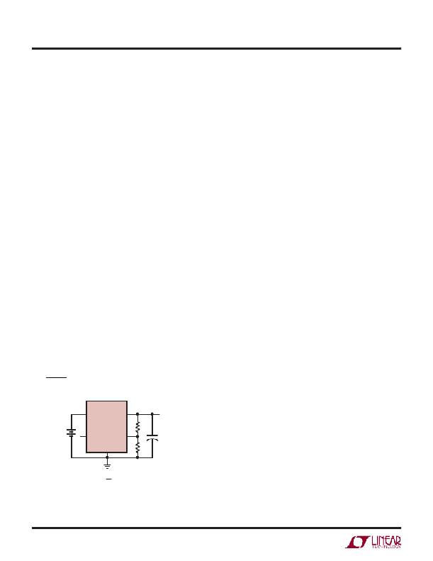
�?� (� )� =� (� )�
�Adjustable Operation�
�The� adjustable� version� of� the� LT1129� has� an� output� voltage�
�range� of� 3.75V� to� 30V.� The� output� voltage� is� set� by� the�
�ratio� of� two� external� resistors� as� shown� in� Figure� 2.� The�
�device� servos� the� output� voltage� to� maintain� the� voltage�
�at� the� adjust� pin� at� 3.75V.� The� current� in� R1� is� then� equal�
�to� 3.75V/R1.� The� current� in� R2� is� equal� to� the� sum� of� the�
�current� in� R1� and� the� adjust� pin� bias� current.� The� adjust�
�pin� bias� current,� 150nA� at� 25°C,� ?ows� through� R2� into� the�
�adjust� pin.� The� output� voltage� can� be� calculated� according�
�to� the� formula� in� Figure� 2.� The� value� of� R1� should� be� less�
�than� 400k� to� minimize� errors� in� the� output� voltage� caused�
�by� the� adjust� pin� bias� current.� Note� that� in� shutdown� the�
�output� is� turned� off� and� the� divider� current� will� be� zero.�
�Curves� of� Adjust� Pin� Voltage� vs� Temperature� and� Adjust�
�Pin� Bias� Current� vs� Temperature� appear� in� the� Typical�
�Performance� Characteristics.� The� reference� voltage� at�
�the� adjust� pin� has� a� positive� temperature� coef?cient� of�
�approximately� 15ppm/°C.� The� adjust� pin� bias� current� has�
�a� negative� temperature� coef?cient.� These� effects� are� small�
�and� will� tend� to� cancel� each� other.�
�The� adjustable� device� is� speci?ed� with� the� adjust� pin� tied�
�to� the� output� pin.� This� sets� the� output� voltage� to� 3.75V.�
�Speci?cations� for� output� voltages� greater� than� 3.75V� will�
�be� proportional� to� the� ratio� of� the� desired� output� voltage�
�to� 3.75V� (V� OUT� /3.75V).� For� example:� load� regulation� for� an�
�output� current� change� of� 1mA� to� 700mA� is� –� 6mV� typical� at�
�V� OUT� =� 3.75V.� At� V� OUT� =� 12V,� load� regulation� would� be:�
�12V�
�–6mV� –19mV�
�3.75V�
�Thermal� Considerations�
�The� power� handling� capability� of� the� device� will� be� limited�
�by� the� maximum� rated� junction� temperature� (125°C).� The�
�power� dissipated� by� the� device� will� be� made� up� of� two�
�components:�
�1.� Output� current� multiplied� by� the� input/output� voltage�
�differential:� I� OUT� ?� (V� IN� –� V� OUT� ),� and�
�2.� Ground� pin� current� multiplied� by� the� input� voltage:�
�I� GND� ?� V� IN� .�
�The� ground� pin� current� can� be� found� by� examining� the�
�Ground� Pin� Current� curves� in� the� Typical� Performance�
�Characteristics.� Power� dissipation� will� be� equal� to� the�
�sum� of� the� two� components� listed� above.�
�The� LT1129� series� regulators� have� internal� thermal�
�limiting� designed� to� protect� the� device� during� overload�
�conditions.� For� continuous� normal� load� conditions� the�
�maximum� junction� temperature� rating� of� 125°C� must� not�
�be� exceeded.� It� is� important� to� give� careful� consideration�
�to� all� sources� of� thermal� resistance� from� junction� to� ambi-�
�ent.� Additional� heat� sources� mounted� nearby� must� also� be�
�considered.�
�For� surface� mount� devices� heat� sinking� is� accomplished�
�by� using� the� heat� spreading� capabilities� of� the� PC� board�
�and� its� copper� traces.� Experiments� have� shown� that� the�
�heat� spreading� copper� layer� does� not� need� to� be� electri-�
�cally� connected� to� the� tab� of� the� device.� The� PC� material�
�can� be� very� effective� at� transmitting� heat� between� the� pad�
�area,� attached� to� the� tab� of� the� device,� and� a� ground� or�
�power� plane� layer� either� inside� or� on� the� opposite� side� of�
�the� board.� Although� the� actual� thermal� resistance� of� the�
�PC� material� is� high,� the� length/area� ratio� of� the� thermal�
�IN�
�OUT�
�V� OUT�
�resistor� between� layers� is� small.� Copper� board� stiffeners�
�LT1129�
�SHDN�
�GND�
�ADJ�
�R2�
�R1�
�+�
�and� plated� through� holes� can� also� be� used� to� spread� the�
�heat� generated� by� power� devices.�
�The� following� tables� list� thermal� resistances� for� each�
�package.� For� the� TO-220� package,� thermal� resistance�
�(� )�
�(�
�)�
�V� OUT� =� 3.75V� 1� +� +� I� ADJ� ?� R2�
�112935 F02�
�R2�
�R1�
�V� ADJ� =� 3.75V�
�I� ADJ� =� 150nA� at� 25°C�
�OUTPUT� RANGE� =� 3.75V� to� 30V�
�Figure� 2.� Adjustable� Operation�
�is� given� for� junction-to-case� only� since� this� package�
�is� usually� mounted� to� a� heat� sink.� Measured� values� of�
�thermal� resistance� for� several� different� board� sizes� and�
�copper� areas� are� listed� for� each� package.� All� measure-�
�ments� were� taken� in� still� air� on� 3/32"� FR-4� board� with� 1-oz�
�112935ff�
�10�
�相关PDF资料 |
PDF描述 |
|---|---|
| LT1172MJ8#PBF | IC REG MULTI CONFIG ADJ 8CERDIP |
| LT1173CN8-12 | IC REG BUCK BST INV 12V .4A 8DIP |
| LT1175MPQ-5#TRPBF | IC REG LDO -5V .5A DDPAK-5 |
| LT1176CSW#TRPBF | IC REG MULTI CONFIG ADJ 20SOIC |
| LT1182IS#TRPBF | IC SW REG CCFL/LCD CONTRST16SOIC |
相关代理商/技术参数 |
参数描述 |
|---|---|
| LT11-2-FP | 制造商:Thomas & Betts 功能描述:LT11-2 FOOD PROCESSING OUTLET BOX |
| LT1130A | 制造商:LINER 制造商全称:Linear Technology 功能描述:Advanced Low Power 5V RS232 Drivers/Receivers with Small Capacitors |
| LT1130ACN | 制造商:未知厂家 制造商全称:未知厂家 功能描述:Transceiver |
| LT1130ACNW | 功能描述:IC TXRX 5V RS232 LP CAPS 28DIP RoHS:否 类别:集成电路 (IC) >> 接口 - 驱动器,接收器,收发器 系列:- 标准包装:27 系列:- 类型:收发器 驱动器/接收器数:3/3 规程:RS232,RS485 电源电压:4.75 V ~ 5.25 V 安装类型:表面贴装 封装/外壳:28-SOIC(0.295",7.50mm 宽) 供应商设备封装:28-SOIC 包装:管件 |
| LT1130ACNW#PBF | 功能描述:IC TXRX 5V RS232 LP CAPS 28DIP RoHS:是 类别:集成电路 (IC) >> 接口 - 驱动器,接收器,收发器 系列:- 标准包装:27 系列:- 类型:收发器 驱动器/接收器数:3/3 规程:RS232,RS485 电源电压:4.75 V ~ 5.25 V 安装类型:表面贴装 封装/外壳:28-SOIC(0.295",7.50mm 宽) 供应商设备封装:28-SOIC 包装:管件 |
发布紧急采购,3分钟左右您将得到回复。