- 您现在的位置:买卖IC网 > PDF目录2154 > LT1169CS8#TRPBF (Linear Technology)IC OPAMP JFET LONOISE DUAL 8SOIC PDF资料下载
参数资料
| 型号: | LT1169CS8#TRPBF |
| 厂商: | Linear Technology |
| 文件页数: | 12/12页 |
| 文件大小: | 0K |
| 描述: | IC OPAMP JFET LONOISE DUAL 8SOIC |
| 标准包装: | 2,500 |
| 放大器类型: | J-FET |
| 电路数: | 2 |
| 转换速率: | 4.2 V/µs |
| 增益带宽积: | 5.3MHz |
| 电流 - 输入偏压: | 4pA |
| 电压 - 输入偏移: | 600µV |
| 电流 - 电源: | 5.3mA |
| 电压 - 电源,单路/双路(±): | ±4.5 V ~ 20 V |
| 工作温度: | 0°C ~ 70°C |
| 安装类型: | 表面贴装 |
| 封装/外壳: | 8-SOIC(0.154",3.90mm 宽) |
| 供应商设备封装: | 8-SO |
| 包装: | 带卷 (TR) |
9
LT1169
U
S
A
O
PPLICATI
WU
U
I FOR ATIO
–
+
R2
OUTPUT
RB
CB
R1
CS
RS
CB CS
RB = RS
RS > R1 OR R2
TRANSDUCER
–
+
OUTPUT
CF
CB
RB
CB = CFCS
RB = RFRS
RF
CS
RS
TRANSDUCER
LT1169 F03
Q = CV;
dQ
dt
= I = C
dV
dt
capacitor CB, is used to cancel the phase shift caused by
the op amp input capacitance and RB.
Reduced Power Supply Operation
To take full advantage of a wide input common-mode
range, the LT1169 was designed to eliminate phase rever-
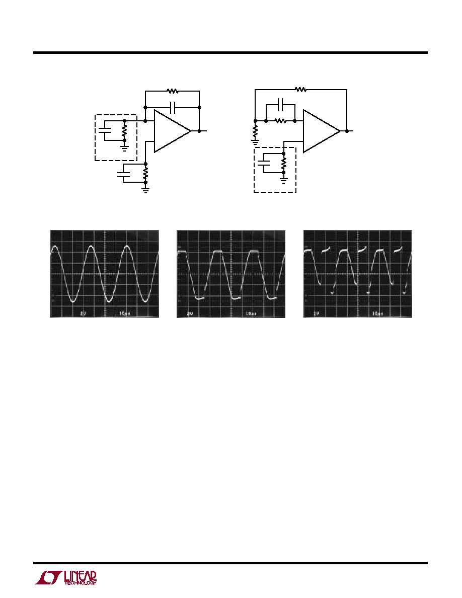
sal. Referring to the photographs in Figure 4, the LT1169
is shown operating in the follower mode (AV = 1) at ±5V
supplies with the input swinging
±5.2V. The output of the
LT1169 clips cleanly and recovers with no phase reversal,
unlike the competition as shown by the last photograph.
This has the benefit of preventing lockup in servo systems
and minimizing distortion components. The effect of input
and output overdrive on one amplifier has no effect on the
other, as each amplifier is biased independently.
Advantages of Matched Dual Op Amps
In many applications the performance of a system
depends on the matching between two operational ampli-
fiers rather than the individual characteristics of the two op
LT1169 Output
Input:
±5.2 Sine Wave
OPA2111 Output
LT1169 F04a
LT1169 F04b
LT1169 F04c
Figure 4. Voltage Follower with Input Exceeding the Common Mode Range (VS = ±5V)
Figure 3. Inverting and Noninverting Gain Configurations
amps. Two or three op amp instrumentation amplifiers,
tracking voltage references and low drift active filters
are some of the circuits requiring matching between two
op amps.
The well-known triple op amp configuration in Figure 5
illustrates these concepts. Output offset is a function of the
difference between the two halves of the LT1169. This error
cancellation principle holds for a considerable
number of input referred parameters in addition to
offset voltage and bias current. Input bias current will
be the average of the two noninverting input currents (IB+).
The difference between these two currents (
IB+)
is the offset current of the instrumentation amplifier. Com-
mon-mode and power supply rejections will be
dependent only on the match between the two amplifiers
(assuming perfect resistor matching).
The concepts of common mode and power supply
rejection ratio match (
CMRR and PSRR) are best dem-
onstrated with a numerical example:
相关PDF资料 |
PDF描述 |
|---|---|
| LT1206CN8 | IC CURRNT FEEDBCK AMP 250MA 8DIP |
| LT1207CS#TRPBF | IC CURRNT FEEDBK AMP DUAL 16SOIC |
| LT1208CS8 | IC OP-AMP HI-SPEED DUAL 8SOIC |
| LT1210CR#TRPBF | IC 35MHZ 1.1 AMP AMPLIFIER 7 DD |
| LT1217CS8#TRPBF | IC CURRNT FEEDBK AMP 10MHZ 8SOIC |
相关代理商/技术参数 |
参数描述 |
|---|---|
| LT117 | 制造商:LINER 制造商全称:Linear Technology 功能描述:Positive Adjustable Regulator |
| LT1170 | 制造商:LINER 制造商全称:Linear Technology 功能描述:100kHz, 5A, 2.5A and 1.25A High Efficiency Switching Regulators |
| LT1170C | 制造商:LINER 制造商全称:Linear Technology 功能描述:100kHz, 5A, 2.5A and 1.25A High Efficiency Switching Regulators |
| LT1170CK | 制造商:Linear Technology 功能描述:Conv DC-DC Single Non-Inv/Inv/Step Up/Step Down 3V to 40V 5-Pin(4+Tab) TO-3 |
| LT1170CQ | 功能描述:IC REG MULTI CONFIG ADJ 5A D2PAK RoHS:否 类别:集成电路 (IC) >> PMIC - 稳压器 - DC DC 开关稳压器 系列:- 设计资源:Design Support Tool 标准包装:1 系列:- 类型:升压(升压) 输出类型:固定 输出数:1 输出电压:3V 输入电压:0.75 V ~ 2 V PWM 型:- 频率 - 开关:- 电流 - 输出:100mA 同步整流器:是 工作温度:-40°C ~ 85°C 安装类型:表面贴装 封装/外壳:SOT-23-5 细型,TSOT-23-5 包装:剪切带 (CT) 供应商设备封装:TSOT-23-5 其它名称:AS1323-BTTT-30CT |
发布紧急采购,3分钟左右您将得到回复。