参数资料
| 型号: | LT1185CT |
| 厂商: | Linear Technology |
| 文件页数: | 3/16页 |
| 文件大小: | 0K |
| 描述: | IC REG LDO NEG ADJ 3A TO220 |
| 标准包装: | 50 |
| 稳压器拓扑结构: | 负,可调式 |
| 输出电压: | -2.5 V ~ -25 V |
| 输入电压: | -4.2 V ~ -35 V |
| 电压 - 压降(标准): | 0.67V @ 3A |
| 稳压器数量: | 1 |
| 电流 - 输出: | 3A |
| 电流 - 限制(最小): | 可调式 |
| 工作温度: | 0°C ~ 70°C |
| 安装类型: | 通孔 |
| 封装/外壳: | TO-220-5 成形引线 |
| 供应商设备封装: | TO-220-5 |
| 包装: | 管件 |
�� �
�
�LT1185�
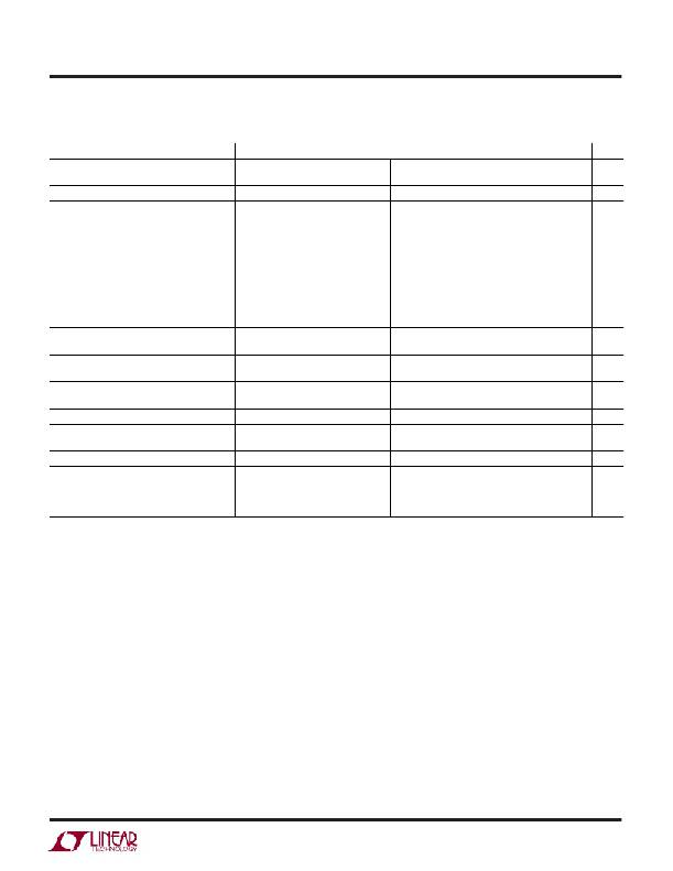
�ELECTRICAL� CHARACTERISTICS�
�The� ●� denotes� specifications� which� apply� over� the� operating� temperature� range,� otherwise� specifications� are� at� T� A� =� 25� °� C.�
�Adjustable� version,� V� IN� =� 7.4V,� V� OUT� =� 5V,� I� OUT� =� 1mA,� R� LIM� =� 4.02k,� unless� otherwise� noted.�
�PARAMETER�
�Load� Regulation� (Note� 7)�
�CONDITIONS�
�I� OUT� =� 5mA� to� 3A�
�MIN�
�TYP�
�0.05�
�MAX�
�0.3�
�UNITS�
�%�
�V� IN� –� V� OUT� =� 1.5V� to� 10V,� V� OUT� =� 5V�
�Line� Regulation� (Note� 7)�
�Minimum� Input� Voltage�
�V� IN� –� V� OUT� =� 1V� to� 20V,� V� OUT� =� 5V�
�I� OUT� =� 1A� (Note� 4),� V� OUT� =� V� REF�
�I� OUT� =� 3A�
�0.002�
�4.0�
�4.3�
�0.01�
�%/V�
�V�
�V�
�Internal� Current� Limit� (See� Graph� for�
�Guaranteed� Curve)� (Note� 12)�
�External� Current� Limit�
�1.5V� ≤� V� IN� –� V� OUT� ≤� 10V�
�V� IN� –� V� OUT� =� 15V�
�V� IN� –� V� OUT� =� 20V�
�V� IN� –� V� OUT� =� 30V�
�5k� ≤� R� LIM� ≤� 15k,� V� OUT� =� 1V�
�●�
�●�
�●�
�●�
�●�
�3.3�
�3.1�
�2.0�
�1.0�
�0.2�
�3.6�
�3.0�
�1.7�
�0.4�
�15k�
�4.2�
�4.4�
�4.2�
�2.6�
�1.0�
�A�
�A�
�A�
�A�
�A�
�A?� ?�
�Programming� Constant�
�(Note� 11)�
�External� Current� Limit� Error�
�Quiescent� Supply� Current�
�Supply� Current� Change� with� Load�
�1A� ≤� I� LIM� ≤� 3A�
�R� LIM� =� 15k� ?� A/I� LIM�
�I� OUT� =� 5mA,� V� OUT� =� V� REF�
�4V� ≤� V� IN� ≤� 25V� (Note� 5)�
�V� IN� –� V� OUT� =� V� SAT� (Note� 10)�
�V� IN� –� V� OUT� ≥� 2V�
�●�
�●�
�●�
�●�
�0.02� I� LIM�
�0.04� I� LIM�
�2.5�
�25�
�10�
�0.06� I� LIM� +� 0.03�
�0.09� I� LIM� +� 0.05�
�3.5�
�40�
�25�
�A�
�A�
�mA�
�mA/A�
�mA/A�
�REF� Pin� Shutoff� Current�
�Thermal� Regulation� (See� Applications�
�V� IN� –� V� OUT� =� 10V�
�●�
�0.4�
�2�
�0.005�
�7�
�0.014�
�μ� A�
�%/W�
�Information)�
�I� OUT� =� 5mA� to� 2A�
�Reference� Voltage� Temperature� Coefficient�
�Thermal� Resistance� Junction� to� Case�
�(Note� 8)�
�TO-3� Control� Area�
�Power� Transistor�
�TO-220� Control� Area�
�Power� Transistor�
�0.003�
�0.01�
�1�
�3�
�1�
�3�
�%/� °� C�
�°� C/W�
�°� C/W�
�°� C/W�
�°� C/W�
�Note� 1:� Stresses� beyond� those� listed� under� Absolute� Maximum� Ratings�
�may� cause� permanent� damage� to� the� device.� Exposure� to� any� Absolute�
�Maximum� Rating� condition� for� extended� periods� may� affect� device�
�reliability� and� lifetime.�
�Note� 2:� Reference� voltage� is� guaranteed� both� at� nominal� conditions� (no�
�load,� 25� °� C)� and� at� worst-case� conditions� of� load,� line,� power� and�
�temperature.� An� intermediate� value� can� be� calculated� by� adding� the� effects�
�of� these� variables� in� the� actual� application.� See� the� Applications�
�Information� section� of� this� data� sheet.�
�Note� 3:� Dropout� voltage� is� tested� by� reducing� input� voltage� until� the�
�output� drops� 1%� below� its� nominal� value.� Tests� are� done� at� 0.5A� and� 3A.�
�The� power� transistor� looks� basically� like� a� pure� resistance� in� this� range� so�
�that� minimum� differential� at� any� intermediate� current� can� be� calculated� by�
�interpolation;� V� DROPOUT� =� 0.25V� +� 0.25� ?� ?� I� OUT� .� For� load� current� less� than�
�0.5A,� see� graph.�
�Note� 4:� “Minimum� input� voltage”� is� limited� by� base� emitter� voltage� drive�
�of� the� power� transistor� section,� not� saturation� as� measured� in� Note� 3.� For�
�output� voltages� below� 4V,� “minimum� input� voltage”� specification� may� limit�
�dropout� voltage� before� transistor� saturation� limitation.�
�Note� 5:� Supply� current� is� measured� on� the� ground� pin,� and� does� not�
�include� load� current,� R� LIM� ,� or� output� divider� current.�
�Note� 6:� The� 25W� power� level� is� guaranteed� for� an� input-output� voltage� of�
�8.3V� to� 17V.� At� lower� voltages� the� 3A� limit� applies,� and� at� higher� voltages�
�the� internal� power� limiting� may� restrict� regulator� power� below� 25W.� See�
�graphs.�
�Note� 7:� Line� and� load� regulation� are� measured� on� a� pulse� basis� with� a�
�pulse� width� of� ≈� 2ms,� to� minimize� heating.� DC� regulation� will� be� affected�
�by� thermal� regulation� and� temperature� coefficient� of� the� reference.� See�
�Applications� Information� section� for� details.�
�Note� 8:� Guaranteed� by� design� and� correlation� to� other� tests,� but� not�
�tested.�
�Note� 9:� T� JMIN� =� 0� °� C� for� the� LT1185C,� –� 40� °� C� for� LT1185I,� and� –55� °� C� for�
�the� LT1185M.� Power� transistor� area� and� control� circuit� area� have� different�
�maximum� junction� temperatures.� Control� area� limits� are� T� JMAX� =� 125� °� C� for�
�the� LT1185C� and� LT1185I� and� 150� °� C� for� the� LT1185M.� Power� area� limits�
�are� 150� °� C� for� LT1185C� and� LT1185I� and� 175� °� C� for� LT1185M.�
�Note� 10:� V� SAT� is� the� maximum� specified� dropout� voltage;�
�0.25V� +� 0.25� ?� I� OUT� .�
�Note� 11:� Current� limit� is� programmed� with� a� resistor� from� REF� pin� to� GND�
�pin.� The� value� is� 15k/I� LIM� .�
�Note� 12:� For� V� IN� –� V� OUT� =� 1.5V;� V� IN� =� 5V,� V� OUT� =� 3.5V.� V� OUT� =� 1V� for� all�
�other� current� limit� tests.�
�1185ff�
�3�
�相关PDF资料 |
PDF描述 |
|---|---|
| MIC37501-1.65WR | IC REG LDO 1.65V SPAK-7 |
| LT3015IMSE-5#TRPBF | IC REG LDO -5V 1.5A 12MSOP |
| ABM18DTMI | CONN EDGECARD 36POS R/A .156 SLD |
| ABM18DTAI | CONN EDGECARD 36POS R/A .156 SLD |
| ABM18DTBI | CONN EDGECARD 36POS R/A .156 SLD |
相关代理商/技术参数 |
参数描述 |
|---|---|
| LT1185CT#06 | 制造商:Linear Technology 功能描述: |
| LT1185CT#06PBF | 制造商:Linear Technology 功能描述:LDO Regulator Neg/Pos 2.5V to 25V-2.5V to -25V 3A 5-Pin(5+Tab) TO-220 制造商:Linear Technology 功能描述:LDO Regulator Neg/Pos -2.5V to -25V2.5V to 25V 3A 5-Pin(5+Tab) TO-220 制造商:Linear Technology 功能描述:IC REG LDO NEG ADJ 3A TO220-5 |
| LT1185CT#30 | 制造商:Linear Technology 功能描述: |
| LT1185CT#30PBF | 制造商:Linear Technology 功能描述:IC REG LDO NEG ADJ 3A TO220-5 |
| LT1185CT#33PBF | 制造商:Linear Technology 功能描述:IC REG LDO NEG ADJ 3A TO220-5 |
发布紧急采购,3分钟左右您将得到回复。