- 您现在的位置:买卖IC网 > PDF目录5942 > LT1219LCS8#TRPBF (Linear Technology)IC PREC OP-AMP R-R IN/OUT 8-SOIC PDF资料下载
参数资料
| 型号: | LT1219LCS8#TRPBF |
| 厂商: | Linear Technology |
| 文件页数: | 1/16页 |
| 文件大小: | 0K |
| 描述: | IC PREC OP-AMP R-R IN/OUT 8-SOIC |
| 标准包装: | 2,500 |
| 系列: | C-Load™ |
| 放大器类型: | 通用 |
| 电路数: | 1 |
| 输出类型: | 满摆幅 |
| 转换速率: | 0.05 V/µs |
| 增益带宽积: | 150kHz |
| 电流 - 输入偏压: | 30nA |
| 电压 - 输入偏移: | 35µV |
| 电流 - 电源: | 400µA |
| 电流 - 输出 / 通道: | 12mA |
| 电压 - 电源,单路/双路(±): | 2 V ~ 10 V,±1 V ~ 5 V |
| 工作温度: | 0°C ~ 70°C |
| 安装类型: | 表面贴装 |
| 封装/外壳: | 8-SOIC(0.154",3.90mm 宽) |
| 供应商设备封装: | 8-SO |
| 包装: | 带卷 (TR) |
1
LT1218/LT1219
s
Rail-to-Rail Input and Output
s
90
V VOS(MAX) for VCM = V– to V+
s
High Common Mode Rejection Ratio: 97dB Min
s
C-Load
TM Stable Version (LT1219)
s
High AVOL: 500V/mV Minimum Driving 10k Load
s
Wide Supply Range:
2V to
±15V (LT1218/LT1219)
2V to
±5V (LT1218L/LT1219L)
s
Shutdown Mode: IS < 30A
s
Low Supply Current: 420
A Max
s
Low Input Bias Current: 18nA Typical
s
300kHz Gain-Bandwidth Product (LT1218)
s
Slew Rate: 0.10V/
s (LT1218)
FEATURES
DESCRIPTION
U
The LT
1218/LT1219 are bipolar op amps which combine
rail-to-rail input and output operation with precision speci-
fications. Unlike other rail-to-rail amplifiers, the LT1218/
LT1219’s input offset voltage is a low 90
V across the
entire rail-to-rail input range, not just a portion of it. Using
a patented technique, both input stages of the LT1218/
LT1219 are trimmed: one at the negative supply and the
other at the positive supply. The resulting common mode
rejection of 97dB minimum is much better than other rail-
to-rail input op amps. A minimum open-loop gain of
500V/mV into a 10k load virtually eliminates all gain error.
The LT1218 has conventional compensation which
assures stability for capacitive loads of 1000pF or less.
The LT1219 has compensation that requires the use of a
0.1
F output capacitor, which improves the amplifier’s
supply rejection and reduces output impedance at high
frequencies. The output capacitor’s filtering action also
reduces high frequency noise, which is beneficial when
driving A/D converters.
High and low voltage versions of the devices are offered.
Operation is specified for 3V, 5V and
±5V supplies for the
LT1218L/LT1219L and 3V, 5V and
±15V for the LT1218/
LT1219.
APPLICATIONS
U
s
Driving A/D Converters
s
Test Equipment Amplifiers
s
MUX Amplifiers
Precision Rail-to-Rail Input
and Output Op Amps
C-Load is a trademark of Linear Technology Corporation.
, LTC and LT are registered trademarks of Linear Technology Corporation.
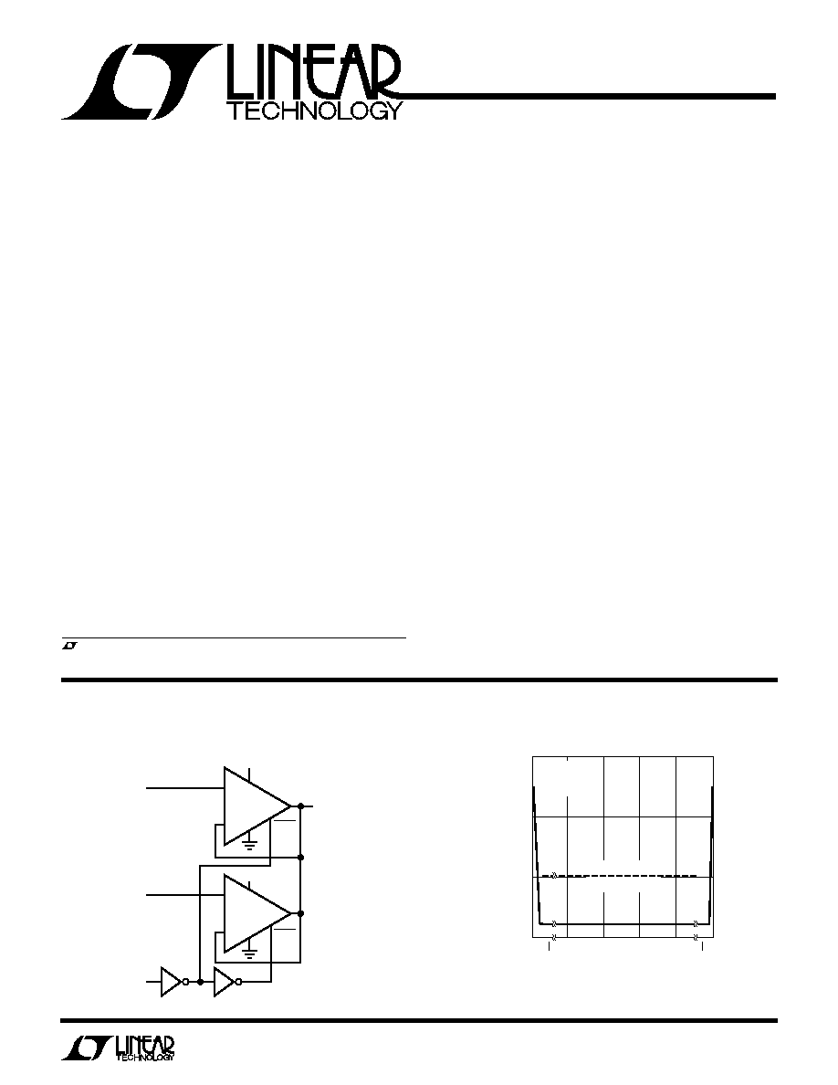
Voltage Follower Input to Output Error
MUX Amplifier
TYPICAL APPLICATION
U
–
+
–
+
LT1218L
VOUT
VIN1
VIN2
INPUT
SELECT
5V
74HCO4
1218/19 TA01
SHDN
MAXIMUM IN
TO OUT ERROR
= 110
V FOR
0.05V
≤ VIN ≤ 4.8V
RL = 10k
SHDN
INPUT VOLTAGE (V)
0
ERROR
(mV)
123
4
LT1218/19 TA02
5
VS = 5V
AV = 1
NO LOAD
10
1.0
0.1
0.01
0.05
4.95
MAX ERROR = 110
V
0.05V
≤ VIN ≤ 4.8V
相关PDF资料 |
PDF描述 |
|---|---|
| RNCF0603BTE6K49 | RES 6.49K OHM 1/16W 0.1% 0603 |
| 104656-5 | CONN HEADER 50POS .050 VERT SMD |
| MQ 500 | FUSE 500MA 125V FAST AXL BULK MQ |
| MRT 2.5 | FUSE SLOW 250VAC 2.5A RADIAL |
| 1-34070-1 | CONN SPLICE BUTT 16-22AWG RED |
相关代理商/技术参数 |
参数描述 |
|---|---|
| LT121AC62000 | 制造商:Toshiba America Electronic Components 功能描述:12.1" XGA P-SI LED LVDS 285 CD |
| LT121CST33 | 制造商:LT 功能描述:New |
| LT121IZ-3.3 | 制造商:LINER 制造商全称:Linear Technology 功能描述:Micropower Low Dropout Regulators with Shutdown |
| LT121S1-105-W1/EVAL | 制造商:All American Misc. 功能描述: |
| LT1220 | 功能描述:PRINTER THERMAL 58MM 24V BENT RoHS:否 类别:计算机,办公室 - 元件,配件 >> 打印机 系列:LT1220 标准包装:1 系列:Thermomark 类型:台式热敏打印机 技术规格:- 其它名称:THERMOMARK S1.1THERMOMARKS1.1 |
发布紧急采购,3分钟左右您将得到回复。