- 您现在的位置:买卖IC网 > PDF目录14819 > LT1305CS8#PBF (Linear Technology)IC REG BOOST 5V 0.4A 8SOIC PDF资料下载
参数资料
| 型号: | LT1305CS8#PBF |
| 厂商: | Linear Technology |
| 文件页数: | 5/8页 |
| 文件大小: | 0K |
| 描述: | IC REG BOOST 5V 0.4A 8SOIC |
| 标准包装: | 100 |
| 类型: | 升压(升压) |
| 输出类型: | 固定 |
| 输出数: | 1 |
| 输出电压: | 5V |
| 输入电压: | 1.8 V ~ 10 V |
| PWM 型: | Burst Mode? |
| 电流 - 输出: | 400mA |
| 同步整流器: | 无 |
| 工作温度: | 0°C ~ 70°C |
| 安装类型: | 表面贴装 |
| 封装/外壳: | 8-SOIC(0.154",3.90mm 宽) |
| 包装: | 管件 |
| 供应商设备封装: | 8-SOIC |
| 产品目录页面: | 1326 (CN2011-ZH PDF) |
�� �
�
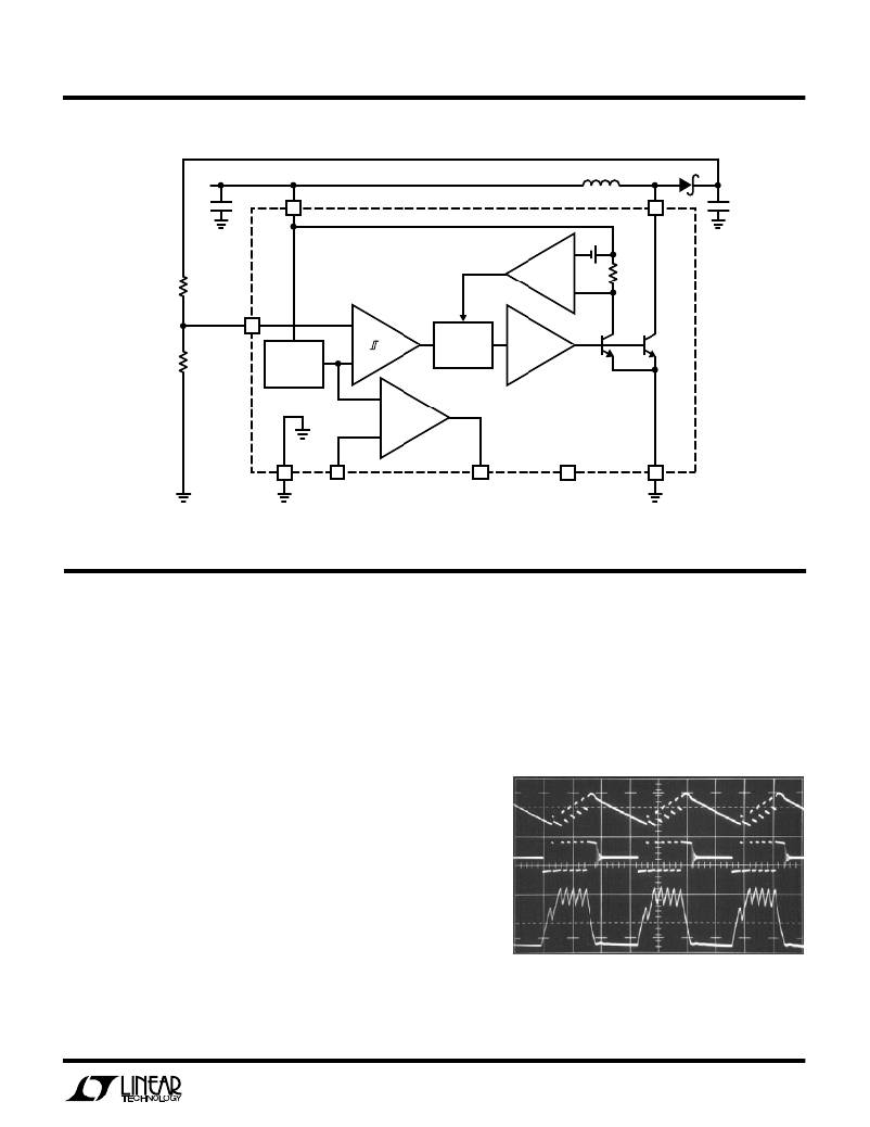
�LT1305�
�BLOCK� DIAGRA� M�
�L1�
�D1�
�V� IN�
�+�
�C5�
�6�
�V� IN�
�7�
�SW�
�+�
�C4�
�CURRENT�
�COMPARATOR�
�36mV�
�R1�
�HYSTERETIC�
�C2�
�R1�
�3� ?�
�COMPARATOR�
�R2�
�4�
�FB�
�REFERENCE�
�1.24V�
�–�
�+�
�C1�
�OFF�
�OSCILLATOR�
�A3�
�DRIVER�
�Q2�
�1� �
�Q1�
�160� �
�–�
�C3�
�+�
�1�
�GND�
�5�
�LBI�
�2�
�LBO�
�SHUTDOWN�
�3�
�8�
�PGND�
�LT1305� ?� F01�
�Figure� 1.� LT1305� Block� Diagram�
�OPERATIO� N�
�Operation� of� the� LT1305� is� best� understood� by� referring� to�
�the� Block� Diagram� in� Figure� 1.� When� C1’s� negative� input,�
�related� to� the� output� voltage� by� the� appropriate� resistor-�
�divider� ratio,� is� higher� than� the� 1.24V� reference� voltage,�
�C1’s� output� is� low.� C2,� A3� and� the� oscillator� are� turned� off,�
�drawing� no� current.� Only� the� reference� and� C1� consume�
�current,� typically� 120� μ� A.� When� C1’s� negative� input� drops�
�below� 1.24V� and� overcomes� C1’s� 6mV� hysteresis,� C1’s�
�output� goes� high,� enabling� the� oscillator,� current� compara-�
�tor� C2� and� driver� A3.� Quiescent� current� increases� to� 2mA�
�as� the� device� goes� into� active� switching� mode.� Q1� then�
�turns� on� in� controlled� saturation� for� nominally� 6� μ� s� or� until�
�current� comparator� C2� trips,� whichever� comes� first.� The�
�switch� then� turns� off� for� approximately� 1.5� μ� s,� then� turns� on�
�again.� The� LT1305’s� switching� causes� current� to� alter-�
�nately� build� up� in� L1� and� dump� into� output� capacitor� C4� via�
�until� V� OUT� decreases� enough� to� force� C1’s� output� high,� and�
�the� entire� cycle� repeats.� Figure� 2� details� relevant� wave-�
�forms.� C1’s� cycling� causes� low-to-mid-frequency� ripple�
�voltage� on� the� output.� Ripple� can� be� reduced� by� making� the�
�output� capacitor� large.� The� 220� μ� F� unit� specified� results� in�
�ripple� of� 50mV� to� 100mV� on� the� 5V� output.� Paralleling� two�
�capacitors� will� decrease� ripple� by� approximately� 50%.�
�V� OUT�
�100mV/DIV�
�AC� COUPLED�
�V� SW�
�5V/DIV�
�I� L�
�1A/DIV�
�D1,� increasing� the� output� voltage.� When� the� output� is� high�
�enough� to� cause� C1’s� output� to� go� high,� switching� action�
�ceases.� Capacitor� C4� is� left� to� supply� current� to� the� load�
�50� μ� s/DIV�
�Figure� 2.� Burst� Mode� Operation�
�LT1305� ?� F02�
�5�
�相关PDF资料 |
PDF描述 |
|---|---|
| LT1054CSW#PBF | IC REG MULTI CONFIG ADJ 16SOIC |
| VI-JVN-EY-F4 | CONVERTER MOD DC/DC 18.5V 50W |
| LT3685EMSE#PBF | IC REG BUCK ADJ 2A 10MSOP |
| LTC3388EMSE-1#PBF | IC REG BUCK SYNC 50MA 10MSOP |
| LTC3523EUD#PBF | IC REG BUCK BOOST SYNC ADJ 16QFN |
相关代理商/技术参数 |
参数描述 |
|---|---|
| LT1306 | 制造商:LINER 制造商全称:Linear Technology 功能描述:Synchronous, Fixed Frequency Step-Up DC/DC Converter |
| LT1306ES8 | 功能描述:IC REG BOOST 5V 1A 8SOIC RoHS:否 类别:集成电路 (IC) >> PMIC - 稳压器 - DC DC 开关稳压器 系列:- 标准包装:2,500 系列:- 类型:降压(降压) 输出类型:固定 输出数:1 输出电压:1.2V,1.5V,1.8V,2.5V 输入电压:2.7 V ~ 20 V PWM 型:- 频率 - 开关:- 电流 - 输出:50mA 同步整流器:是 工作温度:-40°C ~ 125°C 安装类型:表面贴装 封装/外壳:10-TFSOP,10-MSOP(0.118",3.00mm 宽)裸露焊盘 包装:带卷 (TR) 供应商设备封装:10-MSOP 裸露焊盘 |
| LT1306ES8#PBF | 功能描述:IC REG BOOST 5V 1A 8SOIC RoHS:是 类别:集成电路 (IC) >> PMIC - 稳压器 - DC DC 开关稳压器 系列:- 标准包装:2,500 系列:- 类型:降压(降压) 输出类型:固定 输出数:1 输出电压:1.2V,1.5V,1.8V,2.5V 输入电压:2.7 V ~ 20 V PWM 型:- 频率 - 开关:- 电流 - 输出:50mA 同步整流器:是 工作温度:-40°C ~ 125°C 安装类型:表面贴装 封装/外壳:10-TFSOP,10-MSOP(0.118",3.00mm 宽)裸露焊盘 包装:带卷 (TR) 供应商设备封装:10-MSOP 裸露焊盘 |
| LT1306ES8#TR | 功能描述:IC REG BOOST 5V 1A 8SOIC RoHS:否 类别:集成电路 (IC) >> PMIC - 稳压器 - DC DC 开关稳压器 系列:- 标准包装:2,500 系列:- 类型:降压(降压) 输出类型:固定 输出数:1 输出电压:1.2V,1.5V,1.8V,2.5V 输入电压:2.7 V ~ 20 V PWM 型:- 频率 - 开关:- 电流 - 输出:50mA 同步整流器:是 工作温度:-40°C ~ 125°C 安装类型:表面贴装 封装/外壳:10-TFSOP,10-MSOP(0.118",3.00mm 宽)裸露焊盘 包装:带卷 (TR) 供应商设备封装:10-MSOP 裸露焊盘 |
| LT1306ES8#TRPBF | 功能描述:IC REG BOOST 5V 1A 8SOIC RoHS:是 类别:集成电路 (IC) >> PMIC - 稳压器 - DC DC 开关稳压器 系列:- 标准包装:2,500 系列:- 类型:降压(降压) 输出类型:固定 输出数:1 输出电压:1.2V,1.5V,1.8V,2.5V 输入电压:2.7 V ~ 20 V PWM 型:- 频率 - 开关:- 电流 - 输出:50mA 同步整流器:是 工作温度:-40°C ~ 125°C 安装类型:表面贴装 封装/外壳:10-TFSOP,10-MSOP(0.118",3.00mm 宽)裸露焊盘 包装:带卷 (TR) 供应商设备封装:10-MSOP 裸露焊盘 |
发布紧急采购,3分钟左右您将得到回复。