- 您现在的位置:买卖IC网 > PDF目录13913 > LT1374CFE#TRPBF (Linear Technology)IC REG BUCK ADJ 4.5A 16TSSOP PDF资料下载
参数资料
| 型号: | LT1374CFE#TRPBF |
| 厂商: | Linear Technology |
| 文件页数: | 6/32页 |
| 文件大小: | 0K |
| 描述: | IC REG BUCK ADJ 4.5A 16TSSOP |
| 标准包装: | 2,500 |
| 类型: | 降压(降压) |
| 输出类型: | 可调式 |
| 输出数: | 1 |
| 输出电压: | 2.42 V ~ 21.5 V |
| 输入电压: | 5 V ~ 25 V |
| PWM 型: | 电流模式 |
| 频率 - 开关: | 500kHz |
| 电流 - 输出: | 4.5A |
| 同步整流器: | 无 |
| 工作温度: | 0°C ~ 125°C |
| 安装类型: | 表面贴装 |
| 封装/外壳: | 16-TSSOP(0.173",4.40mm)裸露焊盘 |
| 包装: | 带卷 (TR) |
| 供应商设备封装: | 16-TSSOP-EP |
第1页第2页第3页第4页第5页当前第6页第7页第8页第9页第10页第11页第12页第13页第14页第15页第16页第17页第18页第19页第20页第21页第22页第23页第24页第25页第26页第27页第28页第29页第30页第31页第32页
�� �
�
�LT1374�
�TYPICAL� PERFOR� A� CE� CHARACTERISTICS�
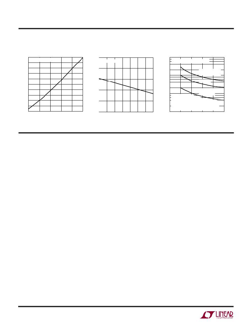
�BOOST� Pin� Current�
�V� C� Pin� Shutdown� Threshold�
�Inductor� Core� Loss�
�100�
�90�
�DUTY� CYCLE� =� 100%�
�1.4�
�SHUTDOWN�
�1.0�
�V� OUT� = 5V, V� IN� = 10V, I� OUT� = 1A�
�20�
�12�
�8�
�80�
�70�
�1.2�
�0.1�
�TYPE� 52�
�POWDERED� IRON�
�4�
�2�
�60�
�50�
�1.0�
�Kool� M� μ�
�?�
�1.2�
�0.8�
�40�
�30�
�20�
�10�
�0.8�
�0.6�
�0.01�
�PERMALLOY�
�μ� =� 125�
�CORE� LOSS� IS�
�INDEPENDENT� OF� LOAD�
�CURRENT� UNTIL� LOAD� CURRENT� FALLS�
�LOW� ENOUGH� FOR� CIRCUIT� TO� GO� INTO�
�0.4�
�0.2�
�0.12�
�0.08�
�0.04�
�0�
�0�
�1�
�2�
�3�
�4�
�5�
�0.4�
�–50�
�–25�
�0�
�25�
�50�
�75�
�100�
�125�
�0.001�
�0�
�DISCONTINUOUS� MODE�
�5� 10� 15�
�20�
�25�
�0.02�
�SWITCH� CURRENT� (A)�
�PI� FU� CTIO� S�
�1374� G16�
�JUNCTION� TEMPERATURE� (� °� C)�
�1374� G11�
�INDUCTANCE� (� μ� H)�
�1374� G01�
�FB/SENSE:� The� feedback� pin� is� the� input� to� the� error�
�amplifier� which� is� referenced� to� an� internal� 2.42V� source.�
�An� external� resistive� divider� is� used� to� set� the� output�
�voltage.� The� fixed� voltage� (-5)� parts� have� the� divider�
�included� on-chip� and� the� FB� pin� is� used� as� a� SENSE� pin,�
�connected� directly� to� the� 5V� output.� Three� additional�
�functions� are� performed� by� the� FB� pin.� When� the� pin�
�voltage� drops� below� 1.7V,� switch� current� limit� is� reduced.�
�Below� 1.5V� the� external� sync� function� is� disabled.� Below�
�1V,� switching� frequency� is� also� reduced.� See� Feedback� Pin�
�Function� section� in� Applications� Information� for� details.�
�BOOST:� The� BOOST� pin� is� used� to� provide� a� drive� voltage,�
�higher� than� the� input� voltage,� to� the� internal� bipolar� NPN�
�power� switch.� Without� this� added� voltage,� the� typical�
�switch� voltage� loss� would� be� about� 1.5V.� The� additional�
�boost� voltage� allows� the� switch� to� saturate� and� voltage�
�loss� approximates� that� of� a� 0.07� ?� FET� structure.� Effi-�
�ciency� improves� from� 75%� for� conventional� bipolar� de-�
�signs� to� >� 89%� for� these� new� parts.�
�V� IN� :� This� is� the� collector� of� the� on-chip� power� NPN� switch.�
�This� pin� powers� the� internal� circuitry� and� internal� regulator�
�when� the� BIAS� pin� is� not� present.� At� NPN� switch� on� and� off,�
�high� dI/dt� edges� occur� on� this� pin.� Keep� the� external�
�bypass� and� catch� diode� close� to� this� pin.� All� trace� induc-�
�tance� on� this� path� will� create� a� voltage� spike� at� switch� off,�
�adding� to� the� V� CE� voltage� across� the� internal� NPN.� Both� V� IN�
�6�
�pins� of� the� 16-lead� TSSOP� package� must� be� shorted�
�together� on� the� PC� board.�
�GND:� The� GND� pin� connection� needs� consideration� for�
�two� reasons.� First,� it� acts� as� the� reference� for� the� regulated�
�output,� so� load� regulation� will� suffer� if� the� “ground”� end� of�
�the� load� is� not� at� the� same� voltage� as� the� GND� pin� of� the�
�IC.� This� condition� will� occur� when� load� current� or� other�
�currents� flow� through� metal� paths� between� the� GND� pin�
�and� the� load� ground� point.� Keep� the� ground� path� short�
�between� the� GND� pin� and� the� load� and� use� a� ground� plane�
�when� possible.� The� second� consideration� is� EMI� caused�
�by� GND� pin� current� spikes.� Internal� capacitance� between�
�the� V� SW� pin� and� the� GND� pin� creates� very� narrow� (<10ns)�
�current� spikes� in� the� GND� pin.� If� the� GND� pin� is� connected�
�to� system� ground� with� a� long� metal� trace,� this� trace� may�
�radiate� excess� EMI.� Keep� the� path� between� the� input�
�bypass� and� the� GND� pin� short.�
�V� SW� :� The� switch� pin� is� the� emitter� of� the� on-chip� power�
�NPN� switch.� This� pin� is� driven� up� to� the� input� pin� voltage�
�during� switch� on� time.� Inductor� current� drives� the� switch�
�pin� negative� during� switch� off� time.� Negative� voltage� is�
�clamped� with� the� external� catch� diode.� Maximum� negative�
�switch� voltage� allowed� is� –� 0.8V.� Both� V� SW� pins� of� the�
�16-lead� TSSOP� package� must� be� shorted� together� on� the�
�PC� board.�
�1374fd�
�相关PDF资料 |
PDF描述 |
|---|---|
| HM77-14004LFTR | LOW PROFILE INDUCTORS |
| EBM36DCCN-S189 | CONN EDGECARD 72POS R/A .156 SLD |
| V300B5C150BG3 | CONVERTER MOD DC/DC 5V 150W |
| EBM36DCCH-S189 | CONN EDGECARD 72POS R/A .156 SLD |
| LTC3413EFE | IC REG BUCK SYNC ADJ 3A 16TSSOP |
相关代理商/技术参数 |
参数描述 |
|---|---|
| LT1374CR | 功能描述:IC REG BUCK ADJ 4.5A D2PAK RoHS:否 类别:集成电路 (IC) >> PMIC - 稳压器 - DC DC 开关稳压器 系列:- 设计资源:Design Support Tool 标准包装:1 系列:- 类型:升压(升压) 输出类型:固定 输出数:1 输出电压:3V 输入电压:0.75 V ~ 2 V PWM 型:- 频率 - 开关:- 电流 - 输出:100mA 同步整流器:是 工作温度:-40°C ~ 85°C 安装类型:表面贴装 封装/外壳:SOT-23-5 细型,TSOT-23-5 包装:剪切带 (CT) 供应商设备封装:TSOT-23-5 其它名称:AS1323-BTTT-30CT |
| LT1374CR#PBF | 功能描述:IC REG BUCK ADJ 4.5A D2PAK RoHS:是 类别:集成电路 (IC) >> PMIC - 稳压器 - DC DC 开关稳压器 系列:- 标准包装:250 系列:- 类型:降压(降压) 输出类型:固定 输出数:1 输出电压:1.2V 输入电压:2.05 V ~ 6 V PWM 型:电压模式 频率 - 开关:2MHz 电流 - 输出:500mA 同步整流器:是 工作温度:-40°C ~ 85°C 安装类型:表面贴装 封装/外壳:6-UFDFN 包装:带卷 (TR) 供应商设备封装:6-SON(1.45x1) 产品目录页面:1032 (CN2011-ZH PDF) 其它名称:296-25628-2 |
| LT1374CR#PBF | 制造商:Linear Technology 功能描述:IC, STEP-DOWN REGULATOR, DPAK-7 |
| LT1374CR#TR | 功能描述:IC REG BUCK ADJ 4.5A D2PAK RoHS:否 类别:集成电路 (IC) >> PMIC - 稳压器 - DC DC 开关稳压器 系列:- 设计资源:Design Support Tool 标准包装:1 系列:- 类型:升压(升压) 输出类型:固定 输出数:1 输出电压:3V 输入电压:0.75 V ~ 2 V PWM 型:- 频率 - 开关:- 电流 - 输出:100mA 同步整流器:是 工作温度:-40°C ~ 85°C 安装类型:表面贴装 封装/外壳:SOT-23-5 细型,TSOT-23-5 包装:剪切带 (CT) 供应商设备封装:TSOT-23-5 其它名称:AS1323-BTTT-30CT |
| LT1374CR#TRPBF | 功能描述:IC REG BUCK ADJ 4.5A D2PAK RoHS:是 类别:集成电路 (IC) >> PMIC - 稳压器 - DC DC 开关稳压器 系列:- 设计资源:Design Support Tool 标准包装:1 系列:- 类型:升压(升压) 输出类型:固定 输出数:1 输出电压:3V 输入电压:0.75 V ~ 2 V PWM 型:- 频率 - 开关:- 电流 - 输出:100mA 同步整流器:是 工作温度:-40°C ~ 85°C 安装类型:表面贴装 封装/外壳:SOT-23-5 细型,TSOT-23-5 包装:剪切带 (CT) 供应商设备封装:TSOT-23-5 其它名称:AS1323-BTTT-30CT |
发布紧急采购,3分钟左右您将得到回复。