- 您现在的位置:买卖IC网 > PDF目录80309 > LT1374IR-5#TRPBF (LINEAR TECHNOLOGY CORP) 8.5 A SWITCHING REGULATOR, 560 kHz SWITCHING FREQ-MAX, PSSO7 PDF资料下载
参数资料
| 型号: | LT1374IR-5#TRPBF |
| 厂商: | LINEAR TECHNOLOGY CORP |
| 元件分类: | 稳压器 |
| 英文描述: | 8.5 A SWITCHING REGULATOR, 560 kHz SWITCHING FREQ-MAX, PSSO7 |
| 封装: | PLASTIC, D2PAK-7 |
| 文件页数: | 11/32页 |
| 文件大小: | 698K |
| 代理商: | LT1374IR-5#TRPBF |
第1页第2页第3页第4页第5页第6页第7页第8页第9页第10页当前第11页第12页第13页第14页第15页第16页第17页第18页第19页第20页第21页第22页第23页第24页第25页第26页第27页第28页第29页第30页第31页第32页
19
LT1374
1374fd
APPLICATIONS INFORMATION
WU
U
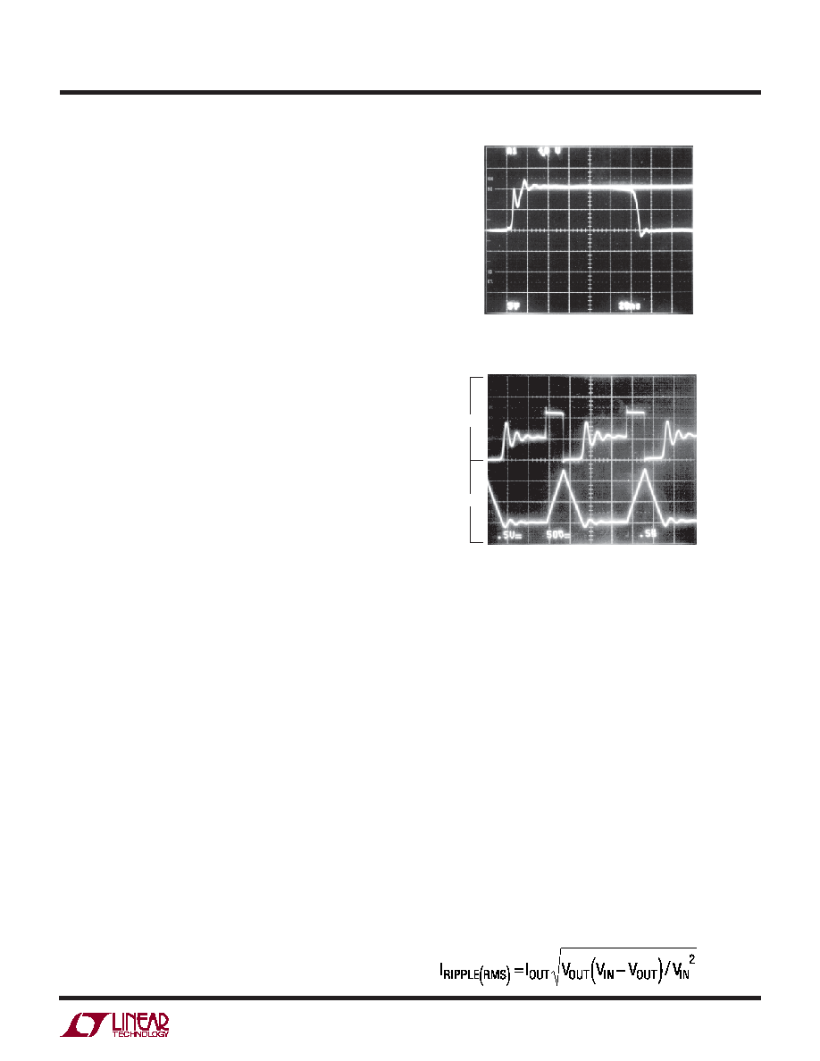
PARASITIC RESONANCE
Resonance or “ringing” may sometimes be seen on the
switch node (see Figure 7). Very high frequency ringing
following switch rise time is caused by switch/diode/input
capacitor lead inductance and diode capacitance. Schot-
tky diodes have very high “Q” junction capacitance that
can ring for many cycles when excited at high frequency.
If total lead length for the input capacitor, diode and switch
path is 1 inch, the inductance will be approximately 25nH.
At switch off, this will produce a spike across the NPN
output device in addition to the input voltage. At higher
currents this spike can be in the order of 10V to 20V or
higher with a poor layout, potentially exceeding the abso-
lute max switch voltage. The path around switch, catch
diode and input capacitor must be kept as short as
possible to ensure reliable operation. When looking at this,
a >100MHz oscilloscope must be used, and waveforms
should be observed on the leads of the package. This
switch off spike will also cause the SW node to go below
ground. The LT1374 has special circuitry inside which
mitigates this problem, but negative voltages over 1V
lasting longer than 10ns should be avoided. Note that
100MHz oscilloscopes are barely fast enough to see the
details of the falling edge overshoot in Figure 7.
A second, much lower frequency ringing is seen during
switch off time if load current is low enough to allow the
inductor current to fall to zero during part of the switch off
time (see Figure 8). Switch and diode capacitance reso-
nate with the inductor to form damped ringing at 1MHz to
10 MHz. This ringing is not harmful to the regulator and it
has not been shown to contribute significantly to EMI. Any
attempt to damp it with a resistive snubber will degrade
efficiency.
INPUT BYPASSING AND VOLTAGE RANGE
Input Bypass Capacitor
Step-down converters draw current from the input supply
in pulses. The average height of these pulses is equal to
load current, and the duty cycle is equal to VOUT/VIN. Rise
and fall time of the current is very fast. A local bypass
capacitor across the input supply is necessary to ensure
proper operation of the regulator and minimize the ripple
current fed back into the input supply.
The capacitor also
forces switching current to flow in a tight local loop,
minimizing EMI.
Do not cheat on the ripple current rating of the Input
bypass capacitor, but also don’t get hung up on the value
in microfarads. The input capacitor is intended to absorb
all the switching current ripple, which can have an RMS
value as high as one half of load current. Ripple current
ratings on the capacitor must be observed to ensure
reliable operation. In many cases it is necessary to parallel
two capacitors to obtain the required ripple rating. Both
capacitors must be of the same value and manufacturer to
guarantee power sharing. The actual value of the capacitor
in microfarads is not particularly important because at
500kHz, any value above 5F is essentially resistive. RMS
ripple current rating is the critical parameter. Actual RMS
current can be calculated from:
5V/DIV
Figure 7. Switch Node Resonance
20ns/DIV
1374 F07
INDUCTOR
CURRENT
20ns/DIV
1375/76 F11
0.5s/DIV
1374 F08
Figure 8. Discontinuous Mode Ringing
5V/DIV
100mA/DIV
SWITCH NODE
VOLTAGE
RISE AND FALL
WAVEFORMS ARE
SUPERIMPOSED
(PULSE WIDTH IS
NOT 120ns)
相关PDF资料 |
PDF描述 |
|---|---|
| LM4051AIX3-1.2+T | 1-OUTPUT TWO TERM VOLTAGE REFERENCE, 1.225 V, PDSO3 |
| LES25A48-1V5REJ | 1-OUTPUT 37.5 W DC-DC REG PWR SUPPLY MODULE |
| LM22674QMRX-ADJ | 0.9 A SWITCHING REGULATOR, 600 kHz SWITCHING FREQ-MAX, PDSO8 |
| LX432CSCT | 1-OUTPUT TWO TERM VOLTAGE REFERENCE, PDSO3 |
| LS5320-9RD4T | 2-OUTPUT 100 W AC-DC PWR FACTOR CORR MODULE |
相关代理商/技术参数 |
参数描述 |
|---|---|
| LT1374IRPBF | 制造商:Linear Technology 功能描述:DC-DC Converter Step-Down 5-25V DDPAK8 |
| LT1374IR-SYNC | 功能描述:IC REG BUCK ADJ 4.5A D2PAK RoHS:否 类别:集成电路 (IC) >> PMIC - 稳压器 - DC DC 开关稳压器 系列:- 设计资源:Design Support Tool 标准包装:1 系列:- 类型:升压(升压) 输出类型:固定 输出数:1 输出电压:3V 输入电压:0.75 V ~ 2 V PWM 型:- 频率 - 开关:- 电流 - 输出:100mA 同步整流器:是 工作温度:-40°C ~ 85°C 安装类型:表面贴装 封装/外壳:SOT-23-5 细型,TSOT-23-5 包装:剪切带 (CT) 供应商设备封装:TSOT-23-5 其它名称:AS1323-BTTT-30CT |
| LT1374IR-SYNC#PBF | 功能描述:IC REG BUCK ADJ 4.5A D2PAK RoHS:是 类别:集成电路 (IC) >> PMIC - 稳压器 - DC DC 开关稳压器 系列:- 设计资源:Design Support Tool 标准包装:1 系列:- 类型:升压(升压) 输出类型:固定 输出数:1 输出电压:3V 输入电压:0.75 V ~ 2 V PWM 型:- 频率 - 开关:- 电流 - 输出:100mA 同步整流器:是 工作温度:-40°C ~ 85°C 安装类型:表面贴装 封装/外壳:SOT-23-5 细型,TSOT-23-5 包装:剪切带 (CT) 供应商设备封装:TSOT-23-5 其它名称:AS1323-BTTT-30CT |
| LT1374IS8 | 功能描述:IC REG BUCK ADJ 4.5A 8SOIC RoHS:否 类别:集成电路 (IC) >> PMIC - 稳压器 - DC DC 开关稳压器 系列:- 设计资源:Design Support Tool 标准包装:1 系列:- 类型:升压(升压) 输出类型:固定 输出数:1 输出电压:3V 输入电压:0.75 V ~ 2 V PWM 型:- 频率 - 开关:- 电流 - 输出:100mA 同步整流器:是 工作温度:-40°C ~ 85°C 安装类型:表面贴装 封装/外壳:SOT-23-5 细型,TSOT-23-5 包装:剪切带 (CT) 供应商设备封装:TSOT-23-5 其它名称:AS1323-BTTT-30CT |
| LT1374IS8#PBF | 功能描述:IC REG BUCK ADJ 4.5A 8SOIC RoHS:是 类别:集成电路 (IC) >> PMIC - 稳压器 - DC DC 开关稳压器 系列:- 设计资源:Design Support Tool 标准包装:1 系列:- 类型:升压(升压) 输出类型:固定 输出数:1 输出电压:3V 输入电压:0.75 V ~ 2 V PWM 型:- 频率 - 开关:- 电流 - 输出:100mA 同步整流器:是 工作温度:-40°C ~ 85°C 安装类型:表面贴装 封装/外壳:SOT-23-5 细型,TSOT-23-5 包装:剪切带 (CT) 供应商设备封装:TSOT-23-5 其它名称:AS1323-BTTT-30CT |
发布紧急采购,3分钟左右您将得到回复。