参数资料
| 型号: | LT1529IT#PBF |
| 厂商: | Linear Technology |
| 文件页数: | 3/12页 |
| 文件大小: | 0K |
| 描述: | IC REG LDO ADJ 3A TO220-5 |
| 产品培训模块: | More Information on LDOs |
| 标准包装: | 50 |
| 稳压器拓扑结构: | 正,可调式 |
| 输出电压: | 3.3 V ~ 14.15 V |
| 输入电压: | 3.8 V ~ 15 V |
| 电压 - 压降(标准): | 0.6V @ 3A |
| 稳压器数量: | 1 |
| 电流 - 输出: | 3A |
| 电流 - 限制(最小): | 3.2A |
| 工作温度: | -45°C ~ 125°C |
| 安装类型: | 通孔 |
| 封装/外壳: | TO-220-5 成形引线 |
| 供应商设备封装: | TO-220-5 |
| 包装: | 管件 |
�� �
�
�LT1529�
�LT1529-3.3/LT1529-5�
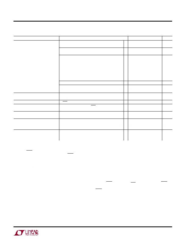
�ELECTRICAL� C� HARA� C� TERISTICS�
�The� ●� denotes� specifications� which� apply� over� the� operating� temperature� range,� otherwise� specificatons� are� at� T� A� =� 25� °� C.� (Note� 3)�
�PARAMETER�
�CONDITIONS�
�MIN�
�TYP�
�MAX�
�UNITS�
�Dropout� Voltage�
�(Note� 6)�
�GND� Pin� Current�
�(Note� 7)�
�I� LOAD� =� 700mA,� T� J� =� 25� °� C�
�I� LOAD� =� 700mA�
�I� LOAD� =� 1.5A,� T� J� =� 25� °� C�
�I� LOAD� =� 1.5A�
�I� LOAD� =� 3A,� T� J� =� 25� °� C�
�I� LOAD� =� 3A�
�I� LOAD� =� 0mA,� T� J� =� 25� °� C�
�I� LOAD� =� 0mA,� T� J� =� 125� °� C� (Note� 8)�
�I� LOAD� =� 100mA,� T� J� =� 25� °� C�
�I� LOAD� =� 100mA,� T� J� =� 125� °� C� (Note� 8)�
�●�
�●�
�●�
�320�
�430�
�600�
�50�
�400�
�0.6�
�1.0�
�430�
�550�
�550�
�700�
�750�
�950�
�100�
�1.0�
�mV�
�mV�
�mV�
�mV�
�mV�
�mV�
�μ� A�
�μ� A�
�mA�
�mA�
�I� LOAD� =� 700mA�
�I� LOAD� =� 1.5A�
�I� LOAD� =� 3A�
�●�
�●�
�●�
�5.5�
�20�
�80�
�12�
�40�
�160�
�mA�
�mA�
�mA�
�ADJ� Pin� Bias� Current� (Notes� 5,� 9)�
�T� J� =� 25� °� C�
�150�
�300�
�nA�
�Shutdown� Threshold�
�SHDN� Pin� Current� (Note� 10)�
�Quiescent� Current� in� Shutdown�
�V� OUT� =� Off� to� On�
�V� OUT� =� On� to� Off�
�V� SHDN� =� 0V�
�V� IN� =� V� OUT� (Nominal)� +� 1V,� V� SHDN� =� 0V�
�●�
�●�
�●�
�●�
�0.25�
�1.20�
�0.75�
�4.5�
�15�
�2.8�
�10�
�30�
�V�
�V�
�μ� A�
�μ� A�
�(Note� 11)�
�Ripple� Rejection�
�V� IN� –� V� OUT� =� 1V� (Avg),� V� RIPPLE� =� 0.5V� P-P� ,�
�50�
�62�
�dB�
�f� RIPPLE� =� 120Hz,� I� LOAD� =� 1.5A�
�Current� Limit�
�V� IN� –� V� OUT� =� 7V,� T� J� =� 25� °� C�
�5�
�A�
�V� IN� =� V� OUT� (Nominal)� +� 1.5V,� ?� V� OUT� =� –� 0.1V�
�●�
�3.2�
�4.7�
�A�
�Input� Reverse� Leakage� Current�
�Reverse� Output� Current� (Note� 12)�
�V� IN� =� –� 15V,� V� OUT� =� 0V�
�LT1529-3.3� V� OUT� =� 3.3V,� V� IN� =� 0V�
�LT1529-5� V� OUT� =� 5V,� V� IN� =� 0V�
�LT1529� (Note� 6)� V� OUT� =� 3.8V,� V� IN� =� 0V�
�●�
�16�
�16�
�16�
�1.0�
�mA�
�μ� A�
�μ� A�
�μ� A�
�Note� 1:� Absolute� Maximum� Ratings� are� those� values� beyond� which� the� life�
�of� a� device� may� be� impaired.�
�Note� 2:� The� SHDN� pin� input� voltage� rating� is� required� for� a� low� impedance�
�source.� Internal� protection� devices� connected� to� the� SHDN� pin� will� turn� on�
�and� clamp� the� pin� to� approximately� 7V� or� –� 0.6V.� This� range� allows� the� use�
�of� 5V� logic� devices� to� drive� the� pin� directly.� For� high� impedance� sources� or�
�logic� running� on� supply� voltages� greater� than� 5.5V,� the� maximum� current�
�driven� into� the� SHDN� pin� must� be� limited� to� less� than� 5mA.�
�Note� 3:� The� device� is� tested� under� pulse� load� conditions� such� that� T� J� =� T� A� .�
�Note� 4:� Operating� conditions� are� limited� by� maximum� junction�
�temperature.� The� regulated� output� voltage� specification� will� not� apply� for�
�all� possible� combinations� of� input� voltage� and� output� current.� When�
�operating� at� maximum� input� voltage,� the� output� current� range� must� be�
�limited.� When� operating� at� maximum� output� current� the� input� voltage�
�range� must� be� limited.�
�Note� 5:� The� LT1529� is� tested� and� specified� with� the� ADJ� pin� connected� to�
�the� OUTPUT� pin.�
�Note� 7:� GND� pin� current� is� tested� with� V� IN� =� V� OUT� (nominal)� and� a� current�
�source� load.� This� means� that� the� device� is� tested� while� operating� in� its�
�dropout� region.� This� is� the� worst-case� GND� pin� current.� The� GND� pin�
�current� will� decrease� slightly� at� higher� input� voltages.�
�Note� 8:� GND� pin� current� will� rise� at� T� J� >� 75� °� C.� This� is� due� to� internal�
�circuitry� designed� to� compensate� for� leakage� currents� in� the� output�
�transistor� at� high� temperatures.� This� allows� quiescent� current� to� be�
�minimized� at� lower� temperatures,� yet� maintain� output� regulation� at� high�
�temperatures� with� light� loads.� See� quiescent� current� curve� in� typical�
�performance� characteristics.�
�Note� 9:� ADJ� pin� bias� current� flows� into� the� ADJ� pin.�
�Note� 10:� SHDN� pin� current� at� V� SHDN� =� 0V� flows� out� of� the� SHDN� pin.�
�Note� 11:� Quiescent� current� in� shutdown� is� equal� to� the� sum� total� of� the�
�SHDN� pin� current� (5� μ� A)� and� the� GND� pin� current� (10� μ� A).�
�Note� 12:� Reverse� output� current� is� tested� with� the� V� IN� pin� grounded� and�
�the� OUTPUT� pin� forced� to� the� rated� output� voltage.� This� current� flows� into�
�the� OUTPUT� pin� and� out� of� the� GND� pin.�
�Note� 6:� Dropout� voltage� is� the� minimum� input/output� voltage� required� to�
�maintain� regulation� at� the� specified� output� current.� In� dropout� the� output�
�voltage� will� be� equal� to� (V� IN� –� V� DROPOUT� ).�
�152935fb�
�3�
�相关PDF资料 |
PDF描述 |
|---|---|
| LT1529IT | IC REG LDO ADJ 3A TO220-5 |
| GMC50DRAS-S734 | CONN EDGECARD 100PS .100 R/A SLD |
| FMC15DRYS-S734 | CONN EDGECARD 30POS DIP .100 SLD |
| LT3015EQ-15#TRPBF | IC REG LDO -15V 1.5A DDPAK5 |
| LT3015EQ-12#TRPBF | IC REG LDO -12V 1.5A DDPAK5 |
相关代理商/技术参数 |
参数描述 |
|---|---|
| LT-1530-110-012 | 制造商:Carling Technologies 功能描述:SINGLE-POLE, LIGHTED TOGGLE, RED LENS - Bulk |
| LT-1530-110-018 | 制造商:Carling Technologies 功能描述:LT-SERIES TOGGLE SWITCH - Bulk |
| LT-1530-610-012 | 制造商:Carling Technologies 功能描述:LT-SERIES TOGGLE SWITCH - Bulk |
| LT-1530-650-012 | 制造商:Carling Technologies 功能描述:LT-SERIES TOGGLE SWITCH - Bulk |
发布紧急采购,3分钟左右您将得到回复。