- 您现在的位置:买卖IC网 > PDF目录377707 > LT1571 (Linear Technology Corporation) Octal Bus Transceivers 20-SOIC 0 to 70 PDF资料下载
参数资料
| 型号: | LT1571 |
| 厂商: | Linear Technology Corporation |
| 英文描述: | Octal Bus Transceivers 20-SOIC 0 to 70 |
| 中文描述: | 恒流/恒压电池充电器预置电压和终止旗 |
| 文件页数: | 12/16页 |
| 文件大小: | 201K |
| 代理商: | LT1571 |
12
LT1571 Series
Figure 10. LT1571 Lead Temperature
instead of V
BAT
(see Figure 8). The optimum boost voltage
(V
X
) is from 3V to 6V.
Then,
P
I
V
V
V
30
V
DRIVER
BAT
BAT
X
X
IN
=
(
)(
)( )
(
+
)
1
55
For example, V
X
= 3.3V,
P
A
V
V
V
V
W
DRIVER
=
(
)(
)(
)
)
+
=
1 2
.
8 4
.
3 3
.
1
3 3
30
55 15
0 045
.
.
The average I
VX
required is:
P
V
X
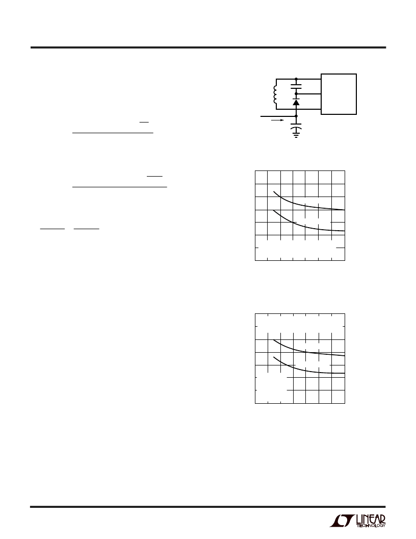
Total board area becomes an important factor when the
area of the board drops below about 20 square inches. The
graph in Figure 9 shows thermal resistance vs board area
for 2-layer and 4-layer boards. Note that 4-layer boards
have significantly lower thermal resistance, but both types
show a rapid increase for reduced board areas. Figure 10
shows actual measured lead temperature for chargers
operating at full current. Battery voltage and input voltage
will affect device power dissipation, so the data sheet
power calculations must be used to extrapolate these
readings to other situations.
Vias should be used to connect board layers together.
Planes under the charger area can be cut away from the
rest of the board and connected with vias to form both a
low thermal resistance system and to act as a ground
plane for reduced EMI.
W
V
mA
DRIVER
=
=
0 045
3 3
.
14
.
Higher Duty Cycle
Maximum duty cycle for the LT1571-1/LT1571-2 is typi-
cally 90% but this may be too low for some applications.
For example, if an 18V
±
3% adapter is used to charge ten
NiMH cells, the charger must put out approximately 15V.
A total of 1.6V is lost in the input diode, switch resistance,
inductor resistance and parasitics so the required duty
Figure 9. LT1571 Thermal Resistance
Figure 8. Lower V
BOOST
BOOST
SW
SENSE
V
X
3V TO 6V
I
VX
1571 F08
LT1571
C1
L1
D2
10
μ
F
+
BOARD AREA (IN
2
)
0
60
55
50
45
40
35
30
25
15
25
1571 F09
5
10
20
30
35
T
°
C
GN16, MEASURED FROM AIR AMBIENT
TO DIE USING COPPER LANDS AS
SHOWN ON DATA SHEET
2-LAYER BOARD
4-LAYER BOARD
BOARD AREA (IN
2
)
0
90
80
70
60
50
40
30
20
15
25
1571 F10
5
10
20
30
35
L
°
C
I
CHRG
= 1.3A
V
IN
V
BAT
= 8.4V
V
BOOST
= V
BAT
T
A
°
C
NOTE: PEAK DIE TEMPERATURE WILL BE
ABOUT 10
°
C HIGHER THAN LEAD TEMPER-
ATURE AT 1.3A CHARGING CURRENT
2-LAYER BOARD
4-LAYER BOARD
cycle is 15/16.4 = 91.4%. The duty cycle can be extended
to 93% by restricting boost voltage to 5V instead of using
V
BAT
as is normally done. This lower boost voltage V
X
(see
Figure 8) also reduces power dissipation in the LT1571.
APPLICATIOU
W
U
U
相关PDF资料 |
PDF描述 |
|---|---|
| LT1572CS | 100kHz, 1.25A Switching Regulator with Catch Diode |
| LT1572 | 100kHz, 1.25A Switching Regulator with Catch Diode(100kHz, 1.25A 开关稳压器(带箝位二极管)) |
| LT1573C | Low Dropout PNP Regulator Driver |
| LT1573CS8 | Low Dropout PNP Regulator Driver |
| LT1573CS8-2.5 | Low Dropout PNP Regulator Driver |
相关代理商/技术参数 |
参数描述 |
|---|---|
| LT1571-1 | 制造商:LINER 制造商全称:Linear Technology 功能描述:Constant-Current/ Constant-Voltage Battery Charger with Preset Voltage and Termination Flag |
| LT-1571-111-012 | 制造商:Carling Technologies 功能描述:LT-SERIES TOGGLE SWITCH - Bulk |
| LT-1571-111-024 | 制造商:Carling Technologies 功能描述:SWITCH, TOGGLE, LTD, SP, 10A, ON-OFF-(ON) 制造商:Carling Technologies 功能描述:LT-SERIES TOGGLE SWITCH - Bulk |
| LT-1571-111-125 | 制造商:Carling Technologies 功能描述:LT-SERIES TOGGLE SWITCH - Bulk |
| LT-1571-112-125 | 制造商:Carling Technologies 功能描述:LT-SERIES TOGGLE SWITCH - Bulk |
发布紧急采购,3分钟左右您将得到回复。