- 您现在的位置:买卖IC网 > PDF目录14170 > LT1616ES6#TRPBF (Linear Technology)IC REG BUCK 3.3V/5V 0.6A SOT23-6 PDF资料下载
参数资料
| 型号: | LT1616ES6#TRPBF |
| 厂商: | Linear Technology |
| 文件页数: | 10/16页 |
| 文件大小: | 0K |
| 描述: | IC REG BUCK 3.3V/5V 0.6A SOT23-6 |
| 标准包装: | 2,500 |
| 类型: | 降压(降压) |
| 输出类型: | 固定 |
| 输出数: | 1 |
| 输出电压: | 3.3V,5V |
| 输入电压: | 3.6 V ~ 25 V |
| PWM 型: | 电流模式 |
| 频率 - 开关: | 1.4MHz |
| 电流 - 输出: | 600mA |
| 同步整流器: | 无 |
| 工作温度: | -40°C ~ 85°C |
| 安装类型: | 表面贴装 |
| 封装/外壳: | SOT-23-6 |
| 包装: | 带卷 (TR) |
| 供应商设备封装: | SOT-23-6 |
�� �
�
�LT1616�
�APPLICATIO� S� I� FOR� ATIO�
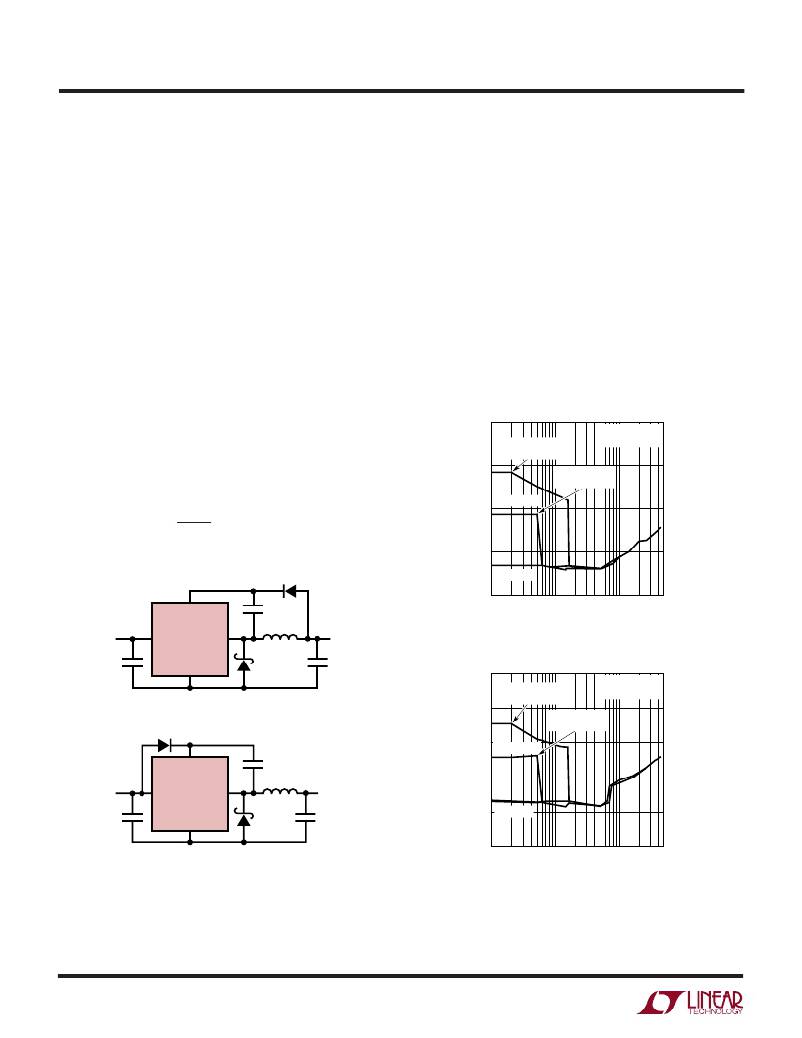
�BOOST� Pin� Considerations�
�Capacitor� C3� and� diode� D2� are� used� to� generate� a� boost�
�voltage� that� is� higher� than� the� input� voltage.� In� most� cases�
�a� 0.01� μ� F� capacitor� and� fast� switching� diode� (such� as� the�
�1N4148� or� 1N914)� will� work� well.� Figure� 5� shows� two�
�ways� to� arrange� the� boost� circuit.� The� BOOST� pin� must� be�
�more� than� 2.5V� above� the� SW� pin� for� best� efficiency.� For�
�outputs� of� 3.3V� and� above,� the� standard� circuit� (Figure� 5a)�
�is� best.� For� outputs� between� 2.8V� and� 3.3V,� use� a� 0.033� μ� F�
�capacitor� and� a� small� Schottky� diode� (such� as� the�
�BAT-54).� For� lower� output� voltages� the� boost� diode� can� be�
�tied� to� the� input� (Figure� 5b).� The� circuit� in� Figure� 5a� is� more�
�efficient� because� the� BOOST� pin� current� comes� from� a�
�charged.� Because� the� boost� capacitor� is� charged� with� the�
�energy� stored� in� the� inductor,� the� circuit� will� rely� on� some�
�minimum� load� current� to� get� the� boost� circuit� running�
�properly.� This� minimum� load� will� depend� on� input� and�
�output� voltages,� and� on� the� arrangement� of� the� boost�
�circuit.� The� minimum� load� generally� goes� to� zero� once� the�
�circuit� has� started.� Figure� 6� shows� a� plot� of� minimum� load�
�to� start� and� to� run� as� a� function� of� input� voltage.� In� many�
�cases� the� discharged� output� capacitor� will� present� a� load�
�to� the� switcher� which� will� allow� it� to� start.� The� plots� show�
�the� worst-case� situation� where� V� IN� is� ramping� very� slowly.�
�Use� a� Schottky� diode� (such� as� the� BAT-54)� for� the� lowest�
�start-up� voltage.�
�D� BOOST� =� BAT54�
�lower voltage source. You must also be sure that the�
�maximum� voltage� rating� of� the� BOOST� pin� is� not� exceeded.�
�The� minimum� operating� voltage� of� an� LT1616� application�
�is� limited� by� the� undervoltage� lockout� (<� 3.6V)� and� by� the�
�maximum� duty� cycle� as� outlined� above.� For� proper� start-�
�up,� the� minimum� input� voltage� is� also� limited� by� the� boost�
�circuit.� If� the� input� voltage� is� ramped� slowly,� or� the� LT1616�
�is� turned� on� with� its� SHDN� pin� when� the� output� is� already�
�7�
�6�
�5�
�Minimum� Input� Voltage� V� OUT� =� 3.3V�
�V� OUT� =� 3.3V�
�BOOST� DIODE�
�TIED� TO� OUTPUT�
�BOOST� DIODE�
�TIED� TO� INPUT�
�V� T� O START�
�in� regulation,� then� the� boost� capacitor� may� not� be� fully�
�D2�
�4�
�3�
�V� TO� RUN�
�BOOST�
�C3�
�1�
�10� 100�
�LOAD� CURRENT� (mA)�
�500�
�V� IN�
�V� IN�
�LT1616�
�SW�
�V� OUT�
�1616� F06a�
�D� BOOST� =� BAT54�
�GND�
�V� BOOST� –� V� SW� ?� V� OUT�
�MAX� V� BOOST� ?� V� IN� +� V� OUT�
�(5a)�
�D2�
�1616� F05a�
�9�
�8�
�7�
�Minimum� Input� Voltage� V� OUT� =� 5V�
�V� OUT� =� 5V�
�BOOST� DIODE�
�TIED� TO� OUTPUT�
�BOOST� DIODE�
�TIED� TO� INPUT�
�V TO START�
�BOOST�
�LT1616�
�C3�
�6�
�V� IN�
�V� IN�
�SW�
�V� OUT�
�5�
�V TO RUN�
�GND�
�V� BOOST� –� V� SW� ?� V� IN�
�MAX� V� BOOST� ?� 2V� IN�
�1616� F05b�
�4�
�1�
�10� 100�
�LOAD� CURRENT� (mA)�
�500�
�(5b)�
�Figure� 5.� Two� Circuits� for� Generating� the� Boost� Voltage�
�1616� F06b�
�Figure� 6.� The� Minimum� Input� Voltage� Depends�
�on� Output� Voltage,� Load� Current� and� Boost� Circuit�
�10�
�相关PDF资料 |
PDF描述 |
|---|---|
| MAX6866UK28D3S+T | IC MPU SUPERVISOR SOT23-5 |
| L-07C1N5SV4T | CER INDUCTOR 1.5NH 0402 |
| L-07C1N2SV4T | CER INDUCTOR 1.2NH 0402 |
| VE-B2M-EX-F2 | CONVERTER MOD DC/DC 10V 75W |
| VE-B2M-EW-F4 | CONVERTER MOD DC/DC 10V 100W |
相关代理商/技术参数 |
参数描述 |
|---|---|
| LT1617 | 制造商:LINER 制造商全称:Linear Technology 功能描述:Inverting Micropower DC/DC Converter with Schottky in ThinSOT Package |
| LT1617-1 | 制造商:LINER 制造商全称:Linear Technology 功能描述:Inverting Micropower DC/DC Converter with Schottky in ThinSOT Package |
| LT1617ES5 | 制造商:LINER 制造商全称:Linear Technology 功能描述:Micropower Inverting DC/DC Converters in SOT-23 |
| LT1617ES5#PBF | 制造商:Linear Technology 功能描述: 制造商:Linear Technology 功能描述:SP-SWREG/Monolithic, CUT TAPE Micropower Inverting DC/DC Converters in SOT-23 制造商:Linear Technology 功能描述:IC, DC/DC CONVERTER, 5-SOT-23, Primary Input Voltage:12V, No. of Outputs:1, Output Voltage:34V, Output Current:350mA, No. of Pins:5, Operating Temperature Min:-40C, Operating Temperature Max:85C, MSL:MSL 1 - Unlimited , RoHS Compliant: Yes |
| LT1617ES5#PBF | 制造商:Linear Technology 功能描述:IC DC/DC CONVERTER 制造商:Linear Technology 功能描述:IC, DC/DC CONVERTER, 5-SOT-23 |
发布紧急采购,3分钟左右您将得到回复。