- 您现在的位置:买卖IC网 > PDF目录14170 > LT1616ES6#TRPBF (Linear Technology)IC REG BUCK 3.3V/5V 0.6A SOT23-6 PDF资料下载
参数资料
| 型号: | LT1616ES6#TRPBF |
| 厂商: | Linear Technology |
| 文件页数: | 12/16页 |
| 文件大小: | 0K |
| 描述: | IC REG BUCK 3.3V/5V 0.6A SOT23-6 |
| 标准包装: | 2,500 |
| 类型: | 降压(降压) |
| 输出类型: | 固定 |
| 输出数: | 1 |
| 输出电压: | 3.3V,5V |
| 输入电压: | 3.6 V ~ 25 V |
| PWM 型: | 电流模式 |
| 频率 - 开关: | 1.4MHz |
| 电流 - 输出: | 600mA |
| 同步整流器: | 无 |
| 工作温度: | -40°C ~ 85°C |
| 安装类型: | 表面贴装 |
| 封装/外壳: | SOT-23-6 |
| 包装: | 带卷 (TR) |
| 供应商设备封装: | SOT-23-6 |
�� �
�
�LT1616�
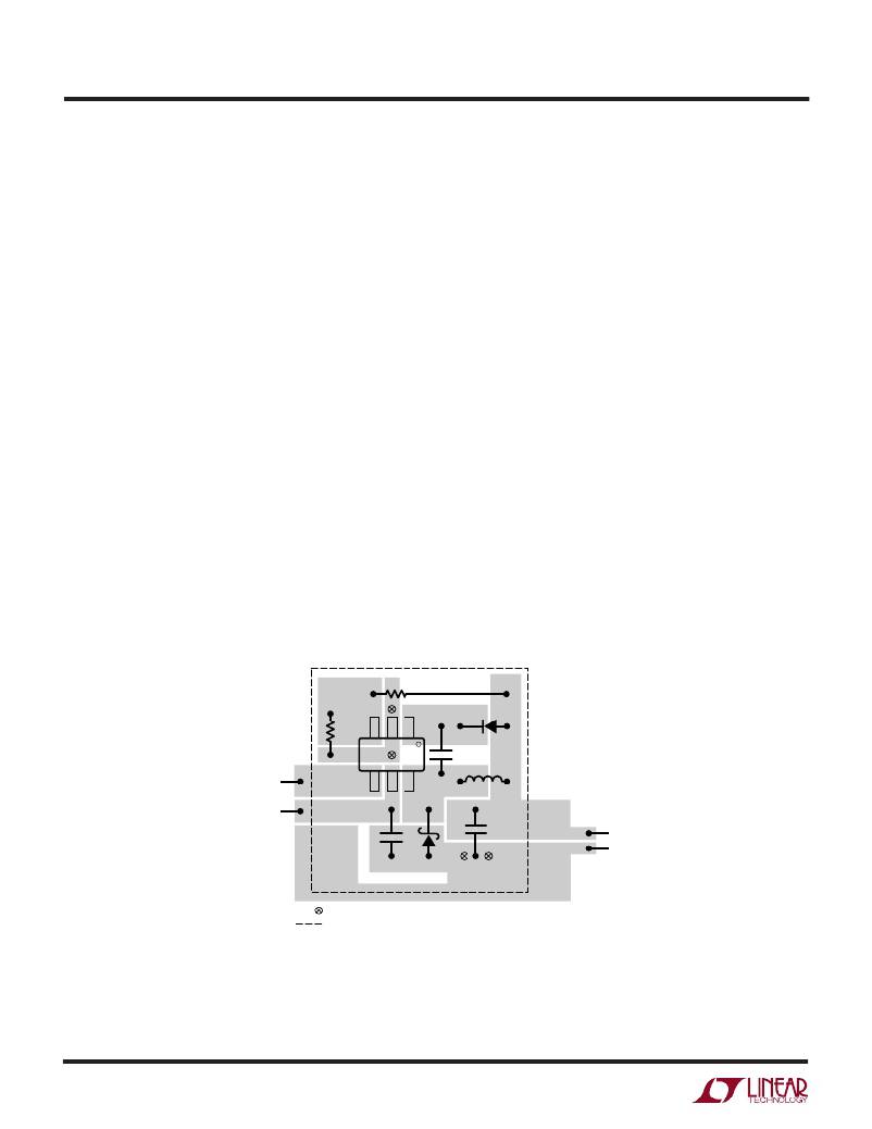
�APPLICATIO� S� I� FOR� ATIO�
�catch� diode� (D1)� and� the� input� capacitor� (C1).� The� loop�
�formed� by� these� components� should� be� as� small� as�
�possible.� Furthermore,� the� system� ground� should� be� tied�
�to� the� regulator� ground� in� only� one� place;� this� prevents� the�
�switched� current� from� injecting� noise� into� the� system�
�ground.� These� components,� along� with� the� inductor� and�
�output� capacitor,� should� be� placed� on� the� same� side� of� the�
�circuit� board,� and� their� connections� should� be� made� on�
�that� layer.� Place� a� local,� unbroken� ground� plane� below�
�these� components,� and� tie� this� ground� plane� to� system�
�ground� at� one� location,� ideally� at� the� ground� terminal� of� the�
�output� capacitor� C2.� Additionally,� the� SW� and� BOOST�
�nodes� should� be� kept� as� small� as� possible.� Finally,� keep�
�the� FB� node� as� small� as� possible� so� that� the� ground� pin� and�
�ground� traces� will� shield� it� from� the� SW� and� BOOST� nodes.�
�Figure� 9� shows� component� placement� with� trace,� ground�
�plane� and� via� locations.� Include� two� vias� near� the� GND� pin�
�of� the� LT1616� to� help� remove� heat� from� the� LT1616� to� the�
�ground� plane.�
�Outputs� Greater� than� 6V�
�For� outputs� greater� than� 6V,� connect� a� diode� (such� as� a�
�1N4148)� from� the� SW� pin� to� V� IN� to� prevent� the� SW� pin�
�from� ringing� above� V� IN� during� discontinuous� mode� opera-�
�tion.� The� 12V� output� circuit� below� shows� the� location� of�
�this� diode.� Also� note� that� for� outputs� above� 10V,� the� input�
�voltage� range� will� be� limited� by� the� maximum� rating� of� the�
�BOOST� pin.� The� 12V� circuit� shows� how� to� overcome� this�
�limitation� using� an� additional� Zener� diode.�
�Other� Linear� Technology� Publications�
�Application� notes� AN19,� AN35� and� AN44� contain� more�
�detailed� descriptions� and� design� information� for� Buck�
�regulators� and� other� switching� regulators.� The� LT1376�
�data� sheet� has� a� more� extensive� discussion� of� output�
�ripple,� loop� compensation� and� stability� testing.� Design�
�Note� DN100� shows� how� to� generate� a� bipolar� output�
�supply� using� a� Buck� regulator.�
�SHUTDOWN�
�V� IN�
�V� OUT�
�SYSTEM�
�GROUND�
�VIAS� TO� LOCAL� GROUND� PLANE�
�1616� F09�
�OUTLINE� OF� LOCAL� GROUND� PLANE�
�Figure� 9.� A� Good� PCB� Layout� Ensures� Proper,� Low� EMI� Operation�
�12�
�相关PDF资料 |
PDF描述 |
|---|---|
| MAX6866UK28D3S+T | IC MPU SUPERVISOR SOT23-5 |
| L-07C1N5SV4T | CER INDUCTOR 1.5NH 0402 |
| L-07C1N2SV4T | CER INDUCTOR 1.2NH 0402 |
| VE-B2M-EX-F2 | CONVERTER MOD DC/DC 10V 75W |
| VE-B2M-EW-F4 | CONVERTER MOD DC/DC 10V 100W |
相关代理商/技术参数 |
参数描述 |
|---|---|
| LT1617 | 制造商:LINER 制造商全称:Linear Technology 功能描述:Inverting Micropower DC/DC Converter with Schottky in ThinSOT Package |
| LT1617-1 | 制造商:LINER 制造商全称:Linear Technology 功能描述:Inverting Micropower DC/DC Converter with Schottky in ThinSOT Package |
| LT1617ES5 | 制造商:LINER 制造商全称:Linear Technology 功能描述:Micropower Inverting DC/DC Converters in SOT-23 |
| LT1617ES5#PBF | 制造商:Linear Technology 功能描述: 制造商:Linear Technology 功能描述:SP-SWREG/Monolithic, CUT TAPE Micropower Inverting DC/DC Converters in SOT-23 制造商:Linear Technology 功能描述:IC, DC/DC CONVERTER, 5-SOT-23, Primary Input Voltage:12V, No. of Outputs:1, Output Voltage:34V, Output Current:350mA, No. of Pins:5, Operating Temperature Min:-40C, Operating Temperature Max:85C, MSL:MSL 1 - Unlimited , RoHS Compliant: Yes |
| LT1617ES5#PBF | 制造商:Linear Technology 功能描述:IC DC/DC CONVERTER 制造商:Linear Technology 功能描述:IC, DC/DC CONVERTER, 5-SOT-23 |
发布紧急采购,3分钟左右您将得到回复。