- 您现在的位置:买卖IC网 > PDF目录10681 > LT1714CGN (Linear Technology)IC COMP R-RINOUT DUAL 16-SSOP PDF资料下载
参数资料
| 型号: | LT1714CGN |
| 厂商: | Linear Technology |
| 文件页数: | 11/16页 |
| 文件大小: | 0K |
| 描述: | IC COMP R-RINOUT DUAL 16-SSOP |
| 标准包装: | 100 |
| 系列: | UltraFast™ |
| 类型: | 带锁销 |
| 元件数: | 2 |
| 输出类型: | CMOS,补充型,满摆幅,TTL |
| 电压 - 电源,单路/双路(±): | 2.4 V ~ 12 V,±2.4 V ~ 6 V |
| 电压 - 输入偏移(最小值): | 4mV @ 5V |
| 电流 - 输入偏压(最小值): | 2µA @ 5V |
| 电流 - 输出(标准): | 20mA |
| 电流 - 静态(最大值): | 7.5mA |
| CMRR, PSRR(标准): | 70dB CMRR,80dB PSRR |
| 传输延迟(最大): | 11ns |
| 磁滞: | 100mV |
| 工作温度: | -40°C ~ 85°C |
| 封装/外壳: | 16-SSOP(0.154",3.90mm 宽) |
| 安装类型: | 表面贴装 |
| 包装: | 管件 |
4
LT1713/LT1714
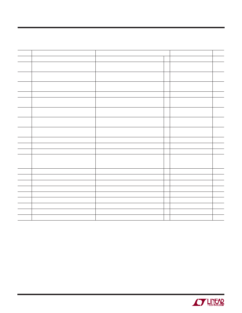
ELECTRICAL CHARACTERISTICS
SYMBOL
PARAMETER
CONDITIONS
MIN
TYP
MAX
UNITS
VCM
Input Voltage Range
q
– 5.1
5.1
V
CMRR
Common Mode Rejection Ratio
– 5V
≤ VCM ≤ 5V
62
70
dB
q
60
dB
PSRR+
Positive Power Supply Rejection Ratio
2.4V
≤ V+ ≤ 7V, VCM = –5V
68
80
dB
q
65
dB
PSRR–
Negative Power Supply Rejection Ratio
– 7V
≤ V– ≤ 0V, VCM = 5V
65
80
dB
q
60
dB
AV
Small-Signal Voltage Gain (Note 10)
1V
≤ VOUT ≤ 4V, RL = ∞
1.5
3
V/mV
VOH
Output Voltage Swing HIGH (Note 8)
IOUT = 1mA, VOVERDRIVE = 50mV
q
4.5
4.8
V
IOUT = 10mA, VOVERDRIVE = 50mV
q
4.3
4.6
V
VOL
Output Voltage Swing LOW (Note 8)
IOUT = – 1mA, VOVERDRIVE = 50mV
q
0.20
0.4
V
IOUT = – 10mA, VOVERDRIVE = 50mV
q
0.35
0.5
V
I+
Positive Supply Current (Per Comparator)
VOVERDRIVE = 1V
5.5
7.5
mA
q
9.0
mA
I–
Negative Supply Current (Per Comparator)
VOVERDRIVE = 1V
3.5
4.5
mA
q
5.0
mA
VIH
Latch Pin High Input Voltage
q
2.4
V
VIL
Latch Pin Low Input Voltage
q
0.8
V
IIL
Latch Pin Current
VLATCH = V+
q
10
A
tPD
Propagation Delay (Note 6)
VIN = 100mV, VOVERDRIVE = 20mV
7
10
ns
VIN = 100mV, VOVERDRIVE = 20mV
q
12
ns
VIN = 100mV, VOVERDRIVE = 5mV
8.5
ns
tPD
Differential Propagation Delay (Note 6)
VIN = 100mV, VOVERDRIVE = 20mV
0.5
3
ns
tr
Output Rise Time
10% to 90%
4
ns
tf
Output Fall Time
90% to 10%
4
ns
tLPD
Latch Propagation Delay (Note 7)
8ns
tSU
Latch Setup Time (Note 7)
1.5
ns
tH
Latch Hold Time (Note 7)
0ns
tDPW
Minimum Latch Disable Pulse Width (Note 7)
8
ns
fMAX
Maximum Toggle Frequency
VIN = 100mVP-P Sine Wave
65
MHz
tJITTER
Output Timing Jitter
VIN = 630mVP-P (0dBm) Sine Wave, f = 30MHz
15
psRMS
The q denotes specifications which apply over the full operating temperature range, otherwise specifications are at TA = 25°C.
V+ = 5V, V– = – 5V, VCM = 0V, VLATCH = 0.8V, CLOAD = 10pF, VOVERDRIVE = 20mV, unless otherwise specified.
Note 1: Absolute Maximum Ratings are those values beyond which the life
of a device may be impaired.
Note 2: The LT1713C/LT1714C are guaranteed to meet specified
performance from 0
°C to 70°C. They are designed, characterized and
expected to meet specified performance from – 40
°C to 85°C but are not
tested or QA sampled at these temperatures. The LT1713I/LT1714I are
guaranteed to meet specified performance from – 40
°C to 85°C.
Note 3: The negative supply should not be greater than the ground pin
voltages and the maximum voltage across the positive and negative
supplies should not be greater than 12V.
Note 4: Input offset voltage (VOS) is defined as the average of the two
voltages measured by forcing first one output, then the other to V+/2.
Note 5: Input bias current (IB) is defined as the average of the two input
currents.
Note 6: Propagation delay (tPD) is measured with the overdrive added to
the actual VOS. Differential propagation delay is defined as:
tPD = tPD+ – tPD–. Load capacitance is 10pF. Due to test system
requirements, the LT1713/LT1714 propagation delay is specified with a
1k
load to ground for ±5V supplies, or to mid-supply for 2.7V or 5V
single supplies.
Note 7: Latch propagation delay (tLPD) is the delay time for the output to
respond when the latch pin is deasserted. Latch setup time (tSU) is the
interval in which the input signal must remain stable prior to asserting the
latch signal. Latch hold time (tH) is the interval after the latch is asserted in
which the input signal must remain stable. Latch disable pulse width
(tDPW) is the width of the negative pulse on the latch enable pin that
latches in new data on the data inputs.
相关PDF资料 |
PDF描述 |
|---|---|
| AD7298BCPZ | IC ADC 12BIT SPI/SRL 1M 20LFCSP |
| VI-24W-MY-B1 | CONVERTER MOD DC/DC 5.5V 50W |
| VE-JWD-MY-F3 | CONVERTER MOD DC/DC 85V 50W |
| VI-23Z-MY-B1 | CONVERTER MOD DC/DC 2V 20W |
| AD7887WARMZ | IC ADC 12BIT 2CH SRL 8-MSOP |
相关代理商/技术参数 |
参数描述 |
|---|---|
| LT1714CGN#PBF | 功能描述:IC COMP R-RINOUT DUAL 16-SSOP RoHS:是 类别:集成电路 (IC) >> 线性 - 比较器 系列:UltraFast™ 标准包装:1 系列:- 类型:通用 元件数:1 输出类型:CMOS,开路集电极,TTL 电压 - 电源,单路/双路(±):2.7 V ~ 5.5 V 电压 - 输入偏移(最小值):7mV @ 5V 电流 - 输入偏压(最小值):0.25µA @ 5V 电流 - 输出(标准):84mA @ 5V 电流 - 静态(最大值):120µA CMRR, PSRR(标准):- 传输延迟(最大):600ns 磁滞:- 工作温度:-40°C ~ 85°C 封装/外壳:SC-74A,SOT-753 安装类型:表面贴装 包装:剪切带 (CT) 产品目录页面:1268 (CN2011-ZH PDF) 其它名称:*LMV331M5*LMV331M5/NOPBLMV331M5CT |
| LT1714CGN#PBF | 制造商:Linear Technology 功能描述:High Speed Comparator IC |
| LT1714CGN#TR | 功能描述:IC COMP R-R I/O DUAL LP 16SSOP RoHS:否 类别:集成电路 (IC) >> 线性 - 比较器 系列:UltraFast™ 产品培训模块:Lead (SnPb) Finish for COTS Obsolescence Mitigation Program 标准包装:2,500 系列:- 类型:通用 元件数:1 输出类型:CMOS,推挽式,满摆幅,TTL 电压 - 电源,单路/双路(±):2.5 V ~ 5.5 V,±1.25 V ~ 2.75 V 电压 - 输入偏移(最小值):5mV @ 5.5V 电流 - 输入偏压(最小值):1pA @ 5.5V 电流 - 输出(标准):- 电流 - 静态(最大值):24µA CMRR, PSRR(标准):80dB CMRR,80dB PSRR 传输延迟(最大):450ns 磁滞:±3mV 工作温度:-40°C ~ 85°C 封装/外壳:6-WFBGA,CSPBGA 安装类型:表面贴装 包装:管件 其它名称:Q3554586 |
| LT1714CGN#TRPBF | 功能描述:IC COMP R-RINOUT DUAL 16-SSOP RoHS:是 类别:集成电路 (IC) >> 线性 - 比较器 系列:UltraFast™ 产品培训模块:Lead (SnPb) Finish for COTS Obsolescence Mitigation Program 标准包装:2,500 系列:- 类型:通用 元件数:1 输出类型:CMOS,推挽式,满摆幅,TTL 电压 - 电源,单路/双路(±):2.5 V ~ 5.5 V,±1.25 V ~ 2.75 V 电压 - 输入偏移(最小值):5mV @ 5.5V 电流 - 输入偏压(最小值):1pA @ 5.5V 电流 - 输出(标准):- 电流 - 静态(最大值):24µA CMRR, PSRR(标准):80dB CMRR,80dB PSRR 传输延迟(最大):450ns 磁滞:±3mV 工作温度:-40°C ~ 85°C 封装/外壳:6-WFBGA,CSPBGA 安装类型:表面贴装 包装:管件 其它名称:Q3554586 |
| LT1714IGN | 功能描述:IC COMP R-RINOUT DUAL 16-SSOP RoHS:否 类别:集成电路 (IC) >> 线性 - 比较器 系列:UltraFast™ 产品培训模块:Lead (SnPb) Finish for COTS Obsolescence Mitigation Program 标准包装:2,500 系列:- 类型:通用 元件数:1 输出类型:CMOS,推挽式,满摆幅,TTL 电压 - 电源,单路/双路(±):2.5 V ~ 5.5 V,±1.25 V ~ 2.75 V 电压 - 输入偏移(最小值):5mV @ 5.5V 电流 - 输入偏压(最小值):1pA @ 5.5V 电流 - 输出(标准):- 电流 - 静态(最大值):24µA CMRR, PSRR(标准):80dB CMRR,80dB PSRR 传输延迟(最大):450ns 磁滞:±3mV 工作温度:-40°C ~ 85°C 封装/外壳:6-WFBGA,CSPBGA 安装类型:表面贴装 包装:管件 其它名称:Q3554586 |
发布紧急采购,3分钟左右您将得到回复。