- 您现在的位置:买卖IC网 > PDF目录377712 > LT1719IS6 (LINEAR TECHNOLOGY CORP) 4.5ns Single/Dual Supply 3V/5V Comparator with Rail-to-Rail Output PDF资料下载
参数资料
| 型号: | LT1719IS6 |
| 厂商: | LINEAR TECHNOLOGY CORP |
| 元件分类: | 运动控制电子 |
| 英文描述: | 4.5ns Single/Dual Supply 3V/5V Comparator with Rail-to-Rail Output |
| 中文描述: | COMPARATOR, 3500 uV OFFSET-MAX, 7 ns RESPONSE TIME, PDSO6 |
| 封装: | PLASTIC, SOT-23, 6 PIN |
| 文件页数: | 12/16页 |
| 文件大小: | 234K |
| 代理商: | LT1719IS6 |
12
LT1719
APPLICATIO
S I
N
FOR
ATIO
U
W
U
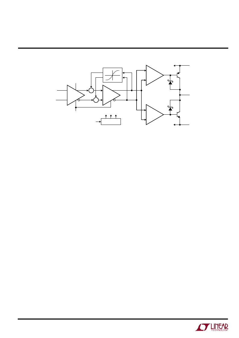
Figure 7. LT1719 Block Diagram
–
+
–
+
–
+
–
+
+IN
–IN
A
V1
V
CC
V
EE
SHUTDOWN
A
V2
NONLINEAR STAGE
OUT
GND
1719 F07
+V
S
+
Σ
+
Σ
BIAS CONTOL
Speed Limits
The LT1719 comparator is intended for high speed appli-
cations, where it is important to understand a few limita-
tions. These limitations can roughly be divided into three
categories: input speed limits, output speed limits, and
internal speed limits.
There are no significant input speed limits except the
shunt capacitance of the input nodes. If the 2pF typical
input nodes are driven, the LT1719 will respond.
The output speed is constrained by two mechanisms, the
first of which is the slew currents available from the output
transistors. To maintain low power quiescent operation,
the LT1719 output transistors are sized to deliver 35mA to
60mA typical slew currents. This is sufficient to drive small
capacitive loads and logic gate inputs at extremely high
speeds. But the slew rate will slow dramatically with heavy
capacitive loads. Because the propagation delay (t
PD
)
definition ends at the time the output voltage is halfway
between the supplies, the fixed slew current makes the
LT1719 faster at 3V than 5V with large capacitive loads and
sufficient input overdrive.
Another manifestation of this output speed limit is skew,
the difference between t
PD+
and t
PD–
. The slew currents of
the LT1719 vary with the process variations of the PNP
and NPN transistors, for rising edges and falling edges
respectively. The typical 0.5ns skew can have either polar-
ity, rising edge or falling edge faster. Again, the skew will
increase dramatically with heavy capacitive loads.
common mode range. The differential input voltage range
is rail-to-rail, without the large input currents found in
competing devices. The input stage also features phase
reversal protection to prevent false outputs when the
inputs are driven below the –100mV common mode
voltage limit.
The internal hysteresis is implemented by positive, nonlin-
ear feedback around a second gain stage. Until this point,
the signal path has been entirely differential. The signal
path is then split into two drive signals for the upper and
lower output transistors. The output transistors are con-
nected common emitter for rail-to-rail output operation.
The Schottky clamps limit the output voltages at about
300mV from the rail, not quite the 50mV or 15mV of Linear
Technology’s rail-to-rail amplifiers and other products.
But the output of a comparator is digital, and this output
stage can drive TTL or CMOS directly. It can also drive ECL,
as described earlier, or analog loads as demonstrated in
the applications to follow.
The bias conditions and signal swings in the output stage
are designed to turn their respective output transistors off
faster than on. This helps minimize the surge of current
from +V
S
to ground that occurs at transitions, to minimize
the frequency-dependent increase in power consumption.
The frequency dependence of the supply current is shown
in the Typical Performance Characteristics.
相关PDF资料 |
PDF描述 |
|---|---|
| LT1721CS | Dual/Quad, 4.5ns, Single Supply 3V/5V Comparators with Rail-to-Rail Outputs |
| LT1721IGN | Dual/Quad, 4.5ns, Single Supply 3V/5V Comparators with Rail-to-Rail Outputs |
| LT1720IS8 | Dual/Quad, 4.5ns, Single Supply 3V/5V Comparators with Rail-to-Rail Outputs |
| LT1720 | Dual/Quad, 4.5ns, Single Supply 3V/5V Comparators with Rail-to-Rail Outputs |
| LT1721 | Dual/Quad, 4.5ns, Single Supply 3V/5V Comparators with Rail-to-Rail Outputs |
相关代理商/技术参数 |
参数描述 |
|---|---|
| LT1719IS6#PBF | 制造商:Linear Technology 功能描述:Comparator Single R-R O/P 制造商:Linear Technology 功能描述:IC ANALOG COMP 1 4.5ns TSOT-23 制造商:Linear Technology 功能描述:IC, ANALOG COMP, 1, 4.5ns, TSOT-23 制造商:Linear Technology 功能描述:IC, ANALOG COMP, 1, 4.5ns, TSOT-23; Comparator Type:High Speed; No. of Comparators:1; Response Time:4.5ns; Supply Voltage Range:2.7V to 6V; Amplifier Case Style:TSOT-23; No. of Pins:6; IC Output Type:CMOS, TTL; Supply Current:4.6mA ;RoHS Compliant: Yes |
| LT1719IS6#TR | 功能描述:IC COMP R-RINOUT SINGLE SOT23-6 RoHS:否 类别:集成电路 (IC) >> 线性 - 比较器 系列:UltraFast™ 标准包装:25 系列:- 类型:带电压基准 元件数:4 输出类型:CMOS,开路漏极,TTL 电压 - 电源,单路/双路(±):2 V ~ 11 V,±1 V ~ 5.5 V 电压 - 输入偏移(最小值):10mV @ 5V 电流 - 输入偏压(最小值):- 电流 - 输出(标准):0.015mA @ 5V 电流 - 静态(最大值):8.5µA CMRR, PSRR(标准):80dB CMRR,80dB PSRR 传输延迟(最大):12µs 磁滞:50mV 工作温度:0°C ~ 70°C 封装/外壳:16-DIP(0.300",7.62mm) 安装类型:通孔 包装:管件 |
| LT1719IS6#TRM | 功能描述:IC COMP R-RINOUT SINGLE SOT23-6 RoHS:否 类别:集成电路 (IC) >> 线性 - 比较器 系列:UltraFast™ 标准包装:25 系列:- 类型:带电压基准 元件数:4 输出类型:CMOS,开路漏极,TTL 电压 - 电源,单路/双路(±):2 V ~ 11 V,±1 V ~ 5.5 V 电压 - 输入偏移(最小值):10mV @ 5V 电流 - 输入偏压(最小值):- 电流 - 输出(标准):0.015mA @ 5V 电流 - 静态(最大值):8.5µA CMRR, PSRR(标准):80dB CMRR,80dB PSRR 传输延迟(最大):12µs 磁滞:50mV 工作温度:0°C ~ 70°C 封装/外壳:16-DIP(0.300",7.62mm) 安装类型:通孔 包装:管件 |
| LT1719IS6#TRMPBF | 功能描述:IC COMP R-RINOUT SINGLE SOT23-6 RoHS:是 类别:集成电路 (IC) >> 线性 - 比较器 系列:UltraFast™ 产品培训模块:Lead (SnPb) Finish for COTS Obsolescence Mitigation Program 标准包装:50 系列:- 类型:带电压基准 元件数:4 输出类型:开路漏极 电压 - 电源,单路/双路(±):2.5 V ~ 11 V,±1.25 V ~ 5.5 V 电压 - 输入偏移(最小值):10mV @ 5V 电流 - 输入偏压(最小值):- 电流 - 输出(标准):0.015mA @ 5V 电流 - 静态(最大值):8.5µA CMRR, PSRR(标准):80dB CMRR,80dB PSRR 传输延迟(最大):- 磁滞:- 工作温度:0°C ~ 70°C 封装/外壳:16-SOIC(0.154",3.90mm 宽) 安装类型:表面贴装 包装:管件 产品目录页面:1386 (CN2011-ZH PDF) |
| LT1719IS6#TRPBF | 功能描述:IC COMP R-RINOUT SINGLE SOT23-6 RoHS:是 类别:集成电路 (IC) >> 线性 - 比较器 系列:UltraFast™ 标准包装:25 系列:- 类型:带电压基准 元件数:4 输出类型:CMOS,开路漏极,TTL 电压 - 电源,单路/双路(±):2 V ~ 11 V,±1 V ~ 5.5 V 电压 - 输入偏移(最小值):10mV @ 5V 电流 - 输入偏压(最小值):- 电流 - 输出(标准):0.015mA @ 5V 电流 - 静态(最大值):8.5µA CMRR, PSRR(标准):80dB CMRR,80dB PSRR 传输延迟(最大):12µs 磁滞:50mV 工作温度:0°C ~ 70°C 封装/外壳:16-DIP(0.300",7.62mm) 安装类型:通孔 包装:管件 |
发布紧急采购,3分钟左右您将得到回复。