- 您现在的位置:买卖IC网 > PDF目录377712 > LT1719IS6 (LINEAR TECHNOLOGY CORP) 4.5ns Single/Dual Supply 3V/5V Comparator with Rail-to-Rail Output PDF资料下载
参数资料
| 型号: | LT1719IS6 |
| 厂商: | LINEAR TECHNOLOGY CORP |
| 元件分类: | 运动控制电子 |
| 英文描述: | 4.5ns Single/Dual Supply 3V/5V Comparator with Rail-to-Rail Output |
| 中文描述: | COMPARATOR, 3500 uV OFFSET-MAX, 7 ns RESPONSE TIME, PDSO6 |
| 封装: | PLASTIC, SOT-23, 6 PIN |
| 文件页数: | 7/16页 |
| 文件大小: | 234K |
| 代理商: | LT1719IS6 |
7
LT1719
APPLICATIO
S I
FOR
ATIO
U
W
U
U
The input stage is protected against damage from large
differential signals, up to and beyond a differential voltage
equal to the supply voltage, limited only by the absolute
maximum currents noted. External input protection cir-
cuitry is only needed if currents would otherwise exceed
these absolute maximums. The internal catch diodes can
conduct current up to these rated maximums without
latchup, even when the supply voltage is at the absolute
maximum rating.
The propagation delay does not increase significantly
when driven with large differential voltages, but with low
levels of overdrive, an apparent increase may be seen with
large source resistances due to an RC delay caused by the
2pF typical input capacitance.
Input Bias Current
Input bias current is measured with both inputs held at 1V.
As with any PNP differential input stage, the LT1719 bias
current flows out of the device. It will go to zero on the
higher of the two inputs and double on the lower of the two
inputs. With more than two diode drops of differential
input voltage, the LT1719’s input protection circuitry
activates, and current out of the lower input will increase
an additional 30% and there will be a small bias current
into the higher of the two input pins, of 4
μ
A or less. See the
Typical Performance curve “Input Current vs Differential
Input Voltage.”
High Speed Design Considerations
Application of high speed comparators is often plagued by
oscillations. The LT1719 has 4mV of internal hysteresis,
which will prevent oscillations as long as parasitic output
to input feedback is kept below 4mV. However, with the
2V/ns slew rate of the LT1719 outputs, a 4mV step can be
created at a 100
input source with only 0.02pF of output
to input coupling. The LT1719’s pinout has been arranged
to minimize problems by placing the sensitive inputs away
from the outputs, shielded by the power rails. The input
and output traces of the circuit board should also be
separated, and the requisite level of isolation is readily
achieved if a topside ground plane runs between the
output and the inputs. For multilayer boards where the
ground plane is internal, a topside ground or supply trace
should be run between the inputs and the output.
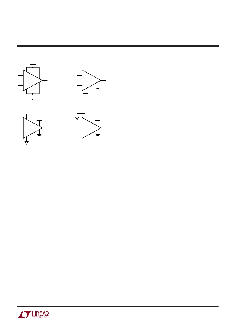
–
+
V
EE
V
CC
2.7V TO 6V
+V
S
GND
Single Supply
–
+
V
EE
V
CC
5V
–5V
3V
+V
S
GND
±
5V
IN
, 3V
OUT
–
+
V
EE
V
CC
10V
5V
+V
S
GND
10V
IN
, 5V
OUT
–
+
V
EE
V
CC
–5.2V
3V
+V
S
GND
1719 F01
Front End Entirely Negative
Figure 1. Variety of Power Supply Configurations
responds correctly to a small differential input signal. If
one input is within the common mode limit, the other input
signal can go outside the common mode limits, up to the
absolute maximum limits, and the output will retain the
correct polarity.
When either input signal falls below the negative common
mode limit, the internal PN diode formed with the sub-
strate can turn on, resulting in significant current flow
through the die. An external Schottky clamp diode
between the input and the negative rail can speed up
recovery from negative overdrive by preventing the sub-
strate diode from turning on.
When both input signals are below the negative common
mode limit, phase reversal protection circuitry prevents
false output inversion to at least –400mV common mode.
However, the offset and hysteresis in this mode will
increase dramatically, to as much as 15mV each. The input
bias currents will also increase.
When both input signals are above the positive common
mode limit, the input stage will get debiased and the output
polarity will be random. However, the internal hysteresis
will hold the output to a valid logic level. When at least one
of the inputs returns to within the common mode limits,
recovery from this state will take as long as 1
μ
s.
相关PDF资料 |
PDF描述 |
|---|---|
| LT1721CS | Dual/Quad, 4.5ns, Single Supply 3V/5V Comparators with Rail-to-Rail Outputs |
| LT1721IGN | Dual/Quad, 4.5ns, Single Supply 3V/5V Comparators with Rail-to-Rail Outputs |
| LT1720IS8 | Dual/Quad, 4.5ns, Single Supply 3V/5V Comparators with Rail-to-Rail Outputs |
| LT1720 | Dual/Quad, 4.5ns, Single Supply 3V/5V Comparators with Rail-to-Rail Outputs |
| LT1721 | Dual/Quad, 4.5ns, Single Supply 3V/5V Comparators with Rail-to-Rail Outputs |
相关代理商/技术参数 |
参数描述 |
|---|---|
| LT1719IS6#PBF | 制造商:Linear Technology 功能描述:Comparator Single R-R O/P 制造商:Linear Technology 功能描述:IC ANALOG COMP 1 4.5ns TSOT-23 制造商:Linear Technology 功能描述:IC, ANALOG COMP, 1, 4.5ns, TSOT-23 制造商:Linear Technology 功能描述:IC, ANALOG COMP, 1, 4.5ns, TSOT-23; Comparator Type:High Speed; No. of Comparators:1; Response Time:4.5ns; Supply Voltage Range:2.7V to 6V; Amplifier Case Style:TSOT-23; No. of Pins:6; IC Output Type:CMOS, TTL; Supply Current:4.6mA ;RoHS Compliant: Yes |
| LT1719IS6#TR | 功能描述:IC COMP R-RINOUT SINGLE SOT23-6 RoHS:否 类别:集成电路 (IC) >> 线性 - 比较器 系列:UltraFast™ 标准包装:25 系列:- 类型:带电压基准 元件数:4 输出类型:CMOS,开路漏极,TTL 电压 - 电源,单路/双路(±):2 V ~ 11 V,±1 V ~ 5.5 V 电压 - 输入偏移(最小值):10mV @ 5V 电流 - 输入偏压(最小值):- 电流 - 输出(标准):0.015mA @ 5V 电流 - 静态(最大值):8.5µA CMRR, PSRR(标准):80dB CMRR,80dB PSRR 传输延迟(最大):12µs 磁滞:50mV 工作温度:0°C ~ 70°C 封装/外壳:16-DIP(0.300",7.62mm) 安装类型:通孔 包装:管件 |
| LT1719IS6#TRM | 功能描述:IC COMP R-RINOUT SINGLE SOT23-6 RoHS:否 类别:集成电路 (IC) >> 线性 - 比较器 系列:UltraFast™ 标准包装:25 系列:- 类型:带电压基准 元件数:4 输出类型:CMOS,开路漏极,TTL 电压 - 电源,单路/双路(±):2 V ~ 11 V,±1 V ~ 5.5 V 电压 - 输入偏移(最小值):10mV @ 5V 电流 - 输入偏压(最小值):- 电流 - 输出(标准):0.015mA @ 5V 电流 - 静态(最大值):8.5µA CMRR, PSRR(标准):80dB CMRR,80dB PSRR 传输延迟(最大):12µs 磁滞:50mV 工作温度:0°C ~ 70°C 封装/外壳:16-DIP(0.300",7.62mm) 安装类型:通孔 包装:管件 |
| LT1719IS6#TRMPBF | 功能描述:IC COMP R-RINOUT SINGLE SOT23-6 RoHS:是 类别:集成电路 (IC) >> 线性 - 比较器 系列:UltraFast™ 产品培训模块:Lead (SnPb) Finish for COTS Obsolescence Mitigation Program 标准包装:50 系列:- 类型:带电压基准 元件数:4 输出类型:开路漏极 电压 - 电源,单路/双路(±):2.5 V ~ 11 V,±1.25 V ~ 5.5 V 电压 - 输入偏移(最小值):10mV @ 5V 电流 - 输入偏压(最小值):- 电流 - 输出(标准):0.015mA @ 5V 电流 - 静态(最大值):8.5µA CMRR, PSRR(标准):80dB CMRR,80dB PSRR 传输延迟(最大):- 磁滞:- 工作温度:0°C ~ 70°C 封装/外壳:16-SOIC(0.154",3.90mm 宽) 安装类型:表面贴装 包装:管件 产品目录页面:1386 (CN2011-ZH PDF) |
| LT1719IS6#TRPBF | 功能描述:IC COMP R-RINOUT SINGLE SOT23-6 RoHS:是 类别:集成电路 (IC) >> 线性 - 比较器 系列:UltraFast™ 标准包装:25 系列:- 类型:带电压基准 元件数:4 输出类型:CMOS,开路漏极,TTL 电压 - 电源,单路/双路(±):2 V ~ 11 V,±1 V ~ 5.5 V 电压 - 输入偏移(最小值):10mV @ 5V 电流 - 输入偏压(最小值):- 电流 - 输出(标准):0.015mA @ 5V 电流 - 静态(最大值):8.5µA CMRR, PSRR(标准):80dB CMRR,80dB PSRR 传输延迟(最大):12µs 磁滞:50mV 工作温度:0°C ~ 70°C 封装/外壳:16-DIP(0.300",7.62mm) 安装类型:通孔 包装:管件 |
发布紧急采购,3分钟左右您将得到回复。