- 您现在的位置:买卖IC网 > PDF目录10792 > LT1720IS8#PBF (Linear Technology)IC COMP R-RINOUT DUAL 8-SOIC PDF资料下载
参数资料
| 型号: | LT1720IS8#PBF |
| 厂商: | Linear Technology |
| 文件页数: | 8/28页 |
| 文件大小: | 0K |
| 描述: | IC COMP R-RINOUT DUAL 8-SOIC |
| 标准包装: | 100 |
| 系列: | UltraFast™ |
| 类型: | 通用 |
| 元件数: | 2 |
| 输出类型: | CMOS,满摆幅,TTL |
| 电压 - 电源,单路/双路(±): | 2.7 V ~ 6 V |
| 电压 - 输入偏移(最小值): | 3mV @ 5V |
| 电流 - 输入偏压(最小值): | 6µA @ 5V |
| 电流 - 输出(标准): | 20mA |
| 电流 - 静态(最大值): | 7mA |
| CMRR, PSRR(标准): | 70dB CMRR,80dB PSRR |
| 传输延迟(最大): | 10ns |
| 磁滞: | 7mV |
| 工作温度: | -40°C ~ 85°C |
| 封装/外壳: | 8-SOIC(0.154",3.90mm 宽) |
| 安装类型: | 表面贴装 |
| 包装: | 管件 |
| 产品目录页面: | 1323 (CN2011-ZH PDF) |
第1页第2页第3页第4页第5页第6页第7页当前第8页第9页第10页第11页第12页第13页第14页第15页第16页第17页第18页第19页第20页第21页第22页第23页第24页第25页第26页第27页第28页
LT1720/LT1721
16
17201fc
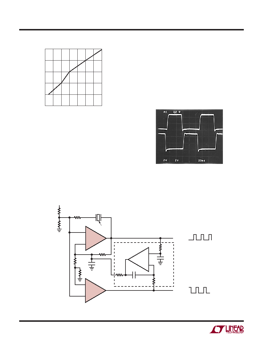
The circuit in Figure 9 shows a crystal oscillator circuit
that generates two nonoverlapping clocks by making full
use of the two independent comparators of the LT1720.
C1 oscillates as before, but with a lower reference level,
C2’s output will toggle at different times. The resistors set
the degree of separation between the output’s high pulses.
With the values shown, each output has a 44% high and
56% low duty cycle, sufcient to allow 2ns between the
high pulses. Figure 10 shows the two outputs.
APPLICATIONS INFORMATION
The optional A1 feedback network shown can be used to
force identical output duty cycles. The steady state duty
cycles of both outputs will be 44%. Note, though, that
the addition of this network only adjusts the percentage
of time each output is high to be the same, which can be
important in switching circuits requiring identical settling
times. It cannot adjust the relative phases between the two
outputs to be exactly 180° apart, because the signal at the
input node driven by the crystal is not a pure sinusoid.
Figure 8. Timing Skew of Figure 7’s Circuit
SUPPLY VOLTAGE (V)
2.5
OUTPUT
SKEW
(ps)
4.5
6.0
1000
800
600
400
200
0
1720/21 F08
3.5
5.5
3.0
4.0
5.0
Figure 10. Nonoverlapping Outputs of Figure 9’s Circuit
Figure 9. Crystal-Based Nonoverlapping 10MHz Clock Generator
–
+
–
+
–
+
C1
1/2 LT1720
C2
1/2 LT1720
A1
LT1636
VCC
2.7V TO 6V
2k
620Ω
220Ω
10MHz
CRYSTAL (AT-CUT)
100k
2.2k
1.3k
2k
1k
17201 F09
0.1μF
OUTPUT 0
OUTPUT 1
GROUND
CASE
OPTIONAL—
SEE TEXT
20ns/DIV
Q1
2V/DIV
Q0
2V/DIV
17201 F10
相关PDF资料 |
PDF描述 |
|---|---|
| AD7538KRZ-REEL | IC DAC 14BIT W/BUFF 24-SOIC |
| VI-242-CU-F2 | CONVERTER MOD DC/DC 15V 200W |
| VI-BN4-MX-F2 | CONVERTER MOD DC/DC 48V 75W |
| VI-240-IW-S | CONVERTER MOD DC/DC 5V 100W |
| VI-BN4-MW | CONVERTER MOD DC/DC 48V 100W |
相关代理商/技术参数 |
参数描述 |
|---|---|
| LT1721 | 制造商:LINER 制造商全称:Linear Technology 功能描述:4ns, 150MHz Dual Comparator with Independent Input/Output Supplies |
| LT1721CGN | 功能描述:IC COMP R-RINOUT QUAD 16-SSOP RoHS:否 类别:集成电路 (IC) >> 线性 - 比较器 系列:UltraFast™ 产品培训模块:Lead (SnPb) Finish for COTS Obsolescence Mitigation Program 标准包装:2,500 系列:- 类型:通用 元件数:1 输出类型:CMOS,推挽式,满摆幅,TTL 电压 - 电源,单路/双路(±):2.5 V ~ 5.5 V,±1.25 V ~ 2.75 V 电压 - 输入偏移(最小值):5mV @ 5.5V 电流 - 输入偏压(最小值):1pA @ 5.5V 电流 - 输出(标准):- 电流 - 静态(最大值):24µA CMRR, PSRR(标准):80dB CMRR,80dB PSRR 传输延迟(最大):450ns 磁滞:±3mV 工作温度:-40°C ~ 85°C 封装/外壳:6-WFBGA,CSPBGA 安装类型:表面贴装 包装:管件 其它名称:Q3554586 |
| LT1721CGN#PBF | 功能描述:IC COMP R-RINOUT QUAD 16-SSOP RoHS:是 类别:集成电路 (IC) >> 线性 - 比较器 系列:UltraFast™ 标准包装:1 系列:- 类型:通用 元件数:1 输出类型:CMOS,开路集电极,TTL 电压 - 电源,单路/双路(±):2.7 V ~ 5.5 V 电压 - 输入偏移(最小值):7mV @ 5V 电流 - 输入偏压(最小值):0.25µA @ 5V 电流 - 输出(标准):84mA @ 5V 电流 - 静态(最大值):120µA CMRR, PSRR(标准):- 传输延迟(最大):600ns 磁滞:- 工作温度:-40°C ~ 85°C 封装/外壳:SC-74A,SOT-753 安装类型:表面贴装 包装:剪切带 (CT) 产品目录页面:1268 (CN2011-ZH PDF) 其它名称:*LMV331M5*LMV331M5/NOPBLMV331M5CT |
| LT1721CGN#PBF | 制造商:Linear Technology 功能描述:High Speed Comparator IC |
| LT1721CGN#TR | 功能描述:IC COMP QUAD R-R 4.5NS 16SSOP RoHS:否 类别:集成电路 (IC) >> 线性 - 比较器 系列:UltraFast™ 产品培训模块:Lead (SnPb) Finish for COTS Obsolescence Mitigation Program 标准包装:2,500 系列:- 类型:通用 元件数:1 输出类型:CMOS,推挽式,满摆幅,TTL 电压 - 电源,单路/双路(±):2.5 V ~ 5.5 V,±1.25 V ~ 2.75 V 电压 - 输入偏移(最小值):5mV @ 5.5V 电流 - 输入偏压(最小值):1pA @ 5.5V 电流 - 输出(标准):- 电流 - 静态(最大值):24µA CMRR, PSRR(标准):80dB CMRR,80dB PSRR 传输延迟(最大):450ns 磁滞:±3mV 工作温度:-40°C ~ 85°C 封装/外壳:6-WFBGA,CSPBGA 安装类型:表面贴装 包装:管件 其它名称:Q3554586 |
发布紧急采购,3分钟左右您将得到回复。