- 您现在的位置:买卖IC网 > PDF目录10043 > LT1739IFE#TRPBF (Linear Technology)IC AMP XDSL LINE DRV DUAL20TSSOP PDF资料下载
参数资料
| 型号: | LT1739IFE#TRPBF |
| 厂商: | Linear Technology |
| 文件页数: | 5/20页 |
| 文件大小: | 0K |
| 描述: | IC AMP XDSL LINE DRV DUAL20TSSOP |
| 标准包装: | 2,500 |
| 类型: | 线路驱动器,发射器 |
| 驱动器/接收器数: | 2/0 |
| 电源电压: | 5 V ~ 12 V |
| 安装类型: | 表面贴装 |
| 封装/外壳: | 20-TSSOP(0.173",4.40mm 宽)裸露焊盘 |
| 供应商设备封装: | 20-TSSOP-EP |
| 包装: | 带卷 (TR) |
13
LT1739
1739fas, sn1739
In differential driver applications, as shown on the first
page of this data sheet, it is recommended that the gain
setting resistor be comprised of two equal value resistors
connected to a good AC ground at high frequencies. This
ensures that the feedback factor of each amplifier remains
less than 0.1 at any frequency. The midpoint of the
resistors can be directly connected to ground, with the
resulting DC gain to the VOS of the amplifiers, or just
bypassed to ground with a 1000pF or larger capacitor.
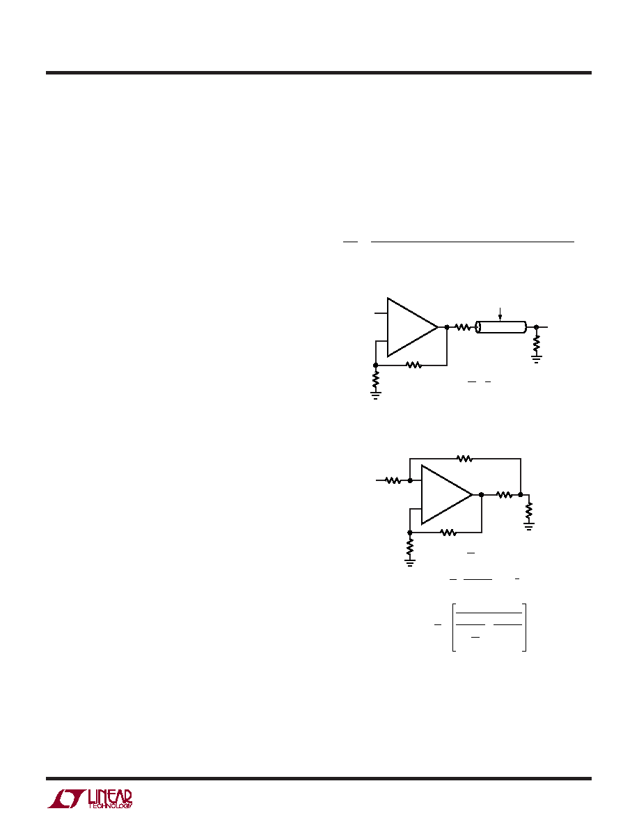
Line Driving Back-Termination
The standard method of cable or line back-termination is
shown in Figure 13. The cable/line is terminated in its
characteristic impedance (50
, 75, 100, 135, etc.).
A back-termination resistor also equal to the chararacteristic
impedance should be used for maximum pulse fidelity of
outgoing signals, and to terminate the line for incoming
signals in a full-duplex application. There are three main
drawbacks to this approach. First, the power dissipated in
the load and back-termination resistors is equal so half of
the power delivered by the amplifier is wasted in the
termination resistor. Second, the signal is halved so the
gain of the amplifer must be doubled to have the same
overall gain to the load. The increase in gain increases
noise and decreases bandwidth (which can also increase
distortion). Third, the output swing of the amplifier is
doubled which can limit the power it can deliver to the load
for a given power supply voltage.
An alternate method of back-termination is shown in
Figure 14. Positive feedback increases the effective back-
termination resistance so RBT can be reduced by a factor
of n. To analyze this circuit, first ground the input. As RBT =
RL/n, and assuming RP2>>RL we require that:
VA = VO (1 – 1/n) to increase the effective value of
RBT by n.
VP = VO (1 – 1/n)/(1 + RF/RG)
VO = VP (1 + RP2/RP1)
APPLICATIO S I FOR ATIO
WU
UU
+
–
1739 F13
RF
RBT
CABLE OR LINE WITH
CHARACTERISTIC IMPEDANCE RL
RG
VO
VI
RL
(1 + RF/RG)
=
VO
VI
1
2
RBT = RL
Figure 13. Standard Cable/Line Back Termination
+
–
1739 F14
RF
RBT
RP2
RP1
RG
VI
VA
VP
VO
RL
RF
RG
1 +
RL
n
=
VO
VI
= 1 –
–
1
n
FOR RBT =
()
RF
RG
1 +
()
RP1
RP1 + RP2
RP1
RP2 + RP1
RP2/(RP2 + RP1)
()
1 + 1/n
Figure 14. Back Termination Using Postive Feedback
Eliminating
VP, we get the following:
(1 + RP2/RP1) = (1 + RF/RG)/(1 – 1/n)
For example, reducing RBT by a factor of n = 4, and with an
amplifer gain of (1 + RF/RG) = 10 requires that RP2/RP1
= 12.3.
Note that the overall gain is increased:
V
RR
R
nR R
R
O
I
PP
P
FG
P
=
+
()
+
() +
()
[]+
()
[]
22
1
12
1
11
1
/
//
/
相关PDF资料 |
PDF描述 |
|---|---|
| IDT72V251L15J | IC FIFO SYNC 4096X18 15NS 32PLCC |
| MS27472E18C32P | CONN RCPT 32POS WALL MT W/PINS |
| IDT72251L25JI | IC FIFO SYNC 512X9 25NS 32PLCC |
| LT1134AIN | IC 4DRV/4RCV RS232 5V 24-DIP |
| VI-2V0-MY | CONVERTER MOD DC/DC 5V 50W |
相关代理商/技术参数 |
参数描述 |
|---|---|
| LT1739IUE | 功能描述:IC AMP XDSL LINE DVR DUAL 12-DFN RoHS:否 类别:集成电路 (IC) >> 接口 - 驱动器,接收器,收发器 系列:- 标准包装:1 系列:- 类型:线路收发器 驱动器/接收器数:5/3 规程:RS232 电源电压:3 V ~ 5.5 V 安装类型:表面贴装 封装/外壳:28-SOIC(0.295",7.50mm 宽) 供应商设备封装:28-SOIC 包装:Digi-Reel® 产品目录页面:918 (CN2011-ZH PDF) 其它名称:296-25096-6 |
| LT1739IUE#TR | 功能描述:IC AMP XDSL LINE DVR DUAL 12-DFN RoHS:否 类别:集成电路 (IC) >> 接口 - 驱动器,接收器,收发器 系列:- 标准包装:27 系列:- 类型:收发器 驱动器/接收器数:3/3 规程:RS232,RS485 电源电压:4.75 V ~ 5.25 V 安装类型:表面贴装 封装/外壳:28-SOIC(0.295",7.50mm 宽) 供应商设备封装:28-SOIC 包装:管件 |
| LT1739IUE#TRPBF | 功能描述:IC AMP XDSL LINE DVR DUAL 12-DFN RoHS:是 类别:集成电路 (IC) >> 接口 - 驱动器,接收器,收发器 系列:- 标准包装:27 系列:- 类型:收发器 驱动器/接收器数:3/3 规程:RS232,RS485 电源电压:4.75 V ~ 5.25 V 安装类型:表面贴装 封装/外壳:28-SOIC(0.295",7.50mm 宽) 供应商设备封装:28-SOIC 包装:管件 |
| LT1740-7 | 制造商:Power-One 功能描述:ACDC - Bulk |
| LT1740-7DZ | 制造商:Power-One 功能描述:ACDC - Bulk |
发布紧急采购,3分钟左右您将得到回复。