参数资料
| 型号: | LT1764AEQ-1.5 |
| 厂商: | Linear Technology |
| 文件页数: | 4/20页 |
| 文件大小: | 0K |
| 描述: | IC REG LDO 1.5V 3A DDPAK-5 |
| 产品培训模块: | More Information on LDOs |
| 标准包装: | 50 |
| 稳压器拓扑结构: | 正,固定式 |
| 输出电压: | 1.5V |
| 输入电压: | 2.7 V ~ 20 V |
| 电压 - 压降(标准): | 0.34V @ 3A |
| 稳压器数量: | 1 |
| 电流 - 输出: | 3A |
| 电流 - 限制(最小): | 3.1A |
| 工作温度: | -40°C ~ 125°C |
| 安装类型: | 表面贴装 |
| 封装/外壳: | TO-263-6,D²Pak(5 引线+接片),TO-263BA |
| 供应商设备封装: | D2PAK-5 |
| 包装: | 管件 |
| 产品目录页面: | 1329 (CN2011-ZH PDF) |
�� �
�
�LT1764A� Series�
�ELECTRICAL� CHARACTERISTICS�
�The� ●� denotes� specifications� which� apply� over� the� full� operating� temperature� range,� otherwise� specifications� are� T� A� =� 25� °� C.� (Note� 2)�
�PARAMETER�
�Current� Limit�
�Input� Reverse� Leakage� Current�
�CONDITIONS�
�V� IN� =� 7V,� V� OUT� =� 0V�
�E� Grade:� LT1764A;� LT1764A-1.5;�
�V� IN� =� 2.7V,� ?� V� OUT� =� –� 0.1V�
�MP� Grade:� LT1764A�
�V� IN� =� 2.8V,� ?� V� OUT� =� –� 0.1V�
�V� IN� =� –� 20V,� V� OUT� =� 0V�
�●�
�●�
�●�
�MIN�
�3.1�
�3.1�
�TYP�
�4�
�MAX�
�1�
�UNITS�
�A�
�A�
�A�
�mA�
�Reverse� Output� Current� (Note� 10)� LT1764A-1.5� V� OUT� =� 1.5V,� V� IN� <� 1.5V�
�LT1764A-1.8� V� OUT� =� 1.8V,� V� IN� <� 1.8V�
�LT1764A-2.5� V� OUT� =� 2.5V,� V� IN� <� 2.5V�
�LT1764A-3.3� V� OUT� =� 3.3V,� V� IN� <� 3.3V�
�LT1764A� (Note� 3)� V� OUT� =� 1.21V,� V� IN� <� 1.21V�
�600�
�600�
�600�
�600�
�300�
�1200�
�1200�
�1200�
�1200�
�600�
�μ� A�
�μ� A�
�μ� A�
�μ� A�
�μ� A�
�Note� 1:� Stresses� beyond� those� listed� under� Absolute� Maximum� Ratings�
�may� cause� permanent� damage� to� the� device.� Exposure� to� any� Absolute�
�Maximum� Rating� condition� for� extended� periods� may� affect� device�
�reliability� and� lifetime.�
�Note� 2:� The� LT1764A� regulators� are� tested� and� specified� under� pulse� load�
�conditions� such� that� T� J� ≈� T� A� .� The� LT1764A� (E� grade)� is� 100%� tested� at�
�T� A� =� 25� °� C;� performance� at� –� 40� °� C� and� 125� °� C� is� assured� by� design,�
�characterization� and� correlation� with� statistical� process� controls.� The�
�LT1764A� (MP� grade)� is� 100%� tested� and� guaranteed� over� the� –55� °� C� to�
�125� °� C� temperature� range.�
�Note� 3:� The� LT1764A� (adjustable� version)� is� tested� and� specified� for� these�
�conditions� with� the� ADJ� pin� connected� to� the� OUT� pin.�
�Note� 4.� Operating� conditions� are� limited� by� maximum� junction� temperature.�
�The� regulated� output� voltage� specification� will� not� apply� for� all� possible�
�combinations� of� input� voltage� and� output� current.� When� operating� at� max-�
�imum� input� voltage,� the� output� current� range� must� be� limited.� When� operat-�
�ing� at� maximum� output� current,� the� input� voltage� range� must� be� limited.�
�Note� 5:� To� satisfy� requirements� for� minimum� input� voltage,� the� LT1764A�
�(adjustable� version)� is� tested� and� specified� for� these� conditions� with� an�
�external� resistor� divider� (two� 4.12k� resistors)� for� an� output� voltage� of�
�2.42V.� The� external� resistor� divider� will� add� a� 300� μ� A� DC� load� on� the� output.�
�Note� 6:� Dropout� voltage� is� the� minimum� input� to� output� voltage� differential�
�needed� to� maintain� regulation� at� a� specified� output� current.� In� dropout,� the�
�output� voltage� will� be� equal� to:� V� IN� –� V� DROPOUT� .�
�Note� 7:� GND� pin� current� is� tested� with� V� IN� =� V� OUT(NOMINAL)� +� 1V� or� V� IN� =�
�2.7V� (E� grade)� or� V� IN� =� 2.8V� (MP� grade),� whichever� is� greater,� and� a� current�
�source� load.� The� GND� pin� current� will� decrease� at� higher� input� voltages.�
�Note� 8:� ADJ� pin� bias� current� flows� into� the� ADJ� pin.�
�Note� 9:� SHDN� pin� current� flows� into� the� SHDN� pin.�
�Note� 10:� Reverse� output� current� is� tested� with� the� IN� pin� grounded� and� the�
�OUT� pin� forced� to� the� rated� output� voltage.� This� current� flows� into� the� OUT�
�pin� and� out� the� GND� pin.�
�Note� 11.� For� the� LT1764A,� LT1764A-1.5� and� LT1764A-1.8� dropout� voltage�
�will� be� limited� by� the� minimum� input� voltage� specification� under� some�
�output� voltage/load� conditions.�
�Note� 12.� All� combinations� of� absolute� maximum� input� voltage� and�
�absolute� maximum� output� voltage� cannot� be� achieved.� The� absolute�
�maximum� differential� from� input� to� output� is� ±� 20V.� For� example,� with�
�V� IN� =� 20V,� V� OUT� cannot� be� pulled� below� ground.�
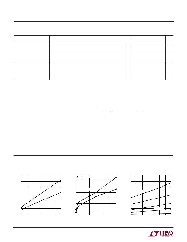
�TYPICAL� PERFOR� A� CE� CHARACTERISTICS�
�Typical� Dropout� Voltage�
�Guaranteed� Dropout� Voltage�
�Dropout� Voltage�
�600�
�500�
�700�
�600�
�=� TEST� POINTS�
�600�
�500�
�400�
�T� J� = 125� °� C�
�500�
�400�
�T� J� ≤� 125� °� C�
�400�
�I� L� =� 3A�
�300�
�300�
�200�
�100�
�T� J� =� 25� °� C�
�300�
�200�
�100�
�T� J� ≤� 25� °� C�
�200�
�100�
�I� L� =� 1.5A�
�I� L� =� 0.5A�
�I� L� = 100mA�
�I� L� =� 1mA�
�0�
�0�
�0.5�
�1.0� 1.5� 2.0�
�2.5�
�3.0�
�0�
�0�
�0.5�
�1.0�
�1.5�
�2.0�
�2.5�
�3.0�
�0�
�–50� –25�
�0�
�25�
�50�
�75�
�100�
�125�
�OUTPUT� CURRENT� (A)�
�1764� G01�
�OUTPUT� CURRENT� (A)�
�1764� G02�
�TEMPERATURE� (� °� C)�
�1764� G03�
�1764afb�
�4�
�相关PDF资料 |
PDF描述 |
|---|---|
| LT1764AEQ | IC REG LDO ADJ 3A DDPAK-5 |
| AMM12DSUI | CONN EDGECARD 24POS .156 DIP SLD |
| AMM12DRUI | CONN EDGECARD 24POS .156 DIP SLD |
| GCB70DHNR | CONN EDGECARD 140PS .050 DIP SLD |
| GBB75DHFR | CONN CARDEDGE 150POS .050" SMD |
相关代理商/技术参数 |
参数描述 |
|---|---|
| LT1764AEQ-2.5 | 功能描述:IC REG LDO 2.5V 3A DDPAK-5 RoHS:否 类别:集成电路 (IC) >> PMIC - 稳压器 - 线性 系列:- 标准包装:1 系列:- 稳压器拓扑结构:正,固定式 输出电压:3V 输入电压:2.3 V ~ 5.5 V 电压 - 压降(标准):0.035V @ 150mA 稳压器数量:2 电流 - 输出:150mA 电流 - 限制(最小):300mA 工作温度:-40°C ~ 125°C 安装类型:表面贴装 封装/外壳:6-UFDFN 裸露焊盘,6-TMLF? 供应商设备封装:6-TMLF?(1.6x1.6) 包装:Digi-Reel® 产品目录页面:1104 (CN2011-ZH PDF) 其它名称:576-3018-6 |
| LT1764AEQ-2.5#PBF | 功能描述:IC REG LDO 2.5V 3A DDPAK-5 RoHS:是 类别:集成电路 (IC) >> PMIC - 稳压器 - 线性 系列:- 标准包装:1 系列:- 稳压器拓扑结构:正,固定式 输出电压:8V 输入电压:10.5 V ~ 23 V 电压 - 压降(标准):1.7V @ 40mA 稳压器数量:1 电流 - 输出:100mA(最小值) 电流 - 限制(最小):- 工作温度:0°C ~ 125°C 安装类型:表面贴装 封装/外壳:8-SOIC(0.154",3.90mm 宽) 供应商设备封装:8-SOIC 包装:剪切带 (CT) 产品目录页面:1075 (CN2011-ZH PDF) 其它名称:296-24390-1 |
| LT1764AEQ-2.5#PBF | 制造商:Linear Technology 功能描述:Linear Voltage Regulator IC 制造商:Linear Technology 功能描述:IC, LDO VOLT REG, 2.5V, 3A, D2-PAK-5 |
| LT1764AEQ-2.5#TR | 功能描述:IC REG LDO 2.5V 3A DDPAK-5 RoHS:否 类别:集成电路 (IC) >> PMIC - 稳压器 - 线性 系列:- 标准包装:1 系列:- 稳压器拓扑结构:正,固定式 输出电压:3V 输入电压:2.3 V ~ 5.5 V 电压 - 压降(标准):0.035V @ 150mA 稳压器数量:2 电流 - 输出:150mA 电流 - 限制(最小):300mA 工作温度:-40°C ~ 125°C 安装类型:表面贴装 封装/外壳:6-UFDFN 裸露焊盘,6-TMLF? 供应商设备封装:6-TMLF?(1.6x1.6) 包装:Digi-Reel® 产品目录页面:1104 (CN2011-ZH PDF) 其它名称:576-3018-6 |
| LT1764AEQ-2.5#TRPBF | 功能描述:IC REG LDO 2.5V 3A DDPAK-5 RoHS:是 类别:集成电路 (IC) >> PMIC - 稳压器 - 线性 系列:- 标准包装:1 系列:- 稳压器拓扑结构:正,固定式 输出电压:3V 输入电压:2.3 V ~ 5.5 V 电压 - 压降(标准):0.035V @ 150mA 稳压器数量:2 电流 - 输出:150mA 电流 - 限制(最小):300mA 工作温度:-40°C ~ 125°C 安装类型:表面贴装 封装/外壳:6-UFDFN 裸露焊盘,6-TMLF? 供应商设备封装:6-TMLF?(1.6x1.6) 包装:Digi-Reel® 产品目录页面:1104 (CN2011-ZH PDF) 其它名称:576-3018-6 |
发布紧急采购,3分钟左右您将得到回复。