- 您现在的位置:买卖IC网 > PDF目录13929 > LT1766EFE-5#TRPBF (Linear Technology)IC REG BUCK 5V 1.5A 16TSSOP PDF资料下载
参数资料
| 型号: | LT1766EFE-5#TRPBF |
| 厂商: | Linear Technology |
| 文件页数: | 7/30页 |
| 文件大小: | 0K |
| 描述: | IC REG BUCK 5V 1.5A 16TSSOP |
| 标准包装: | 2,500 |
| 类型: | 降压(降压) |
| 输出类型: | 固定 |
| 输出数: | 1 |
| 输出电压: | 5V |
| 输入电压: | 5.5 V ~ 60 V |
| PWM 型: | 电流模式 |
| 频率 - 开关: | 200kHz |
| 电流 - 输出: | 1.5A |
| 同步整流器: | 无 |
| 工作温度: | -40°C ~ 125°C |
| 安装类型: | 表面贴装 |
| 封装/外壳: | 16-TSSOP(0.173",4.40mm)裸露焊盘 |
| 包装: | 带卷 (TR) |
| 供应商设备封装: | 16-TSSOP-EP |
第1页第2页第3页第4页第5页第6页当前第7页第8页第9页第10页第11页第12页第13页第14页第15页第16页第17页第18页第19页第20页第21页第22页第23页第24页第25页第26页第27页第28页第29页第30页
�� �
�
�LT1766/LT1766-5�
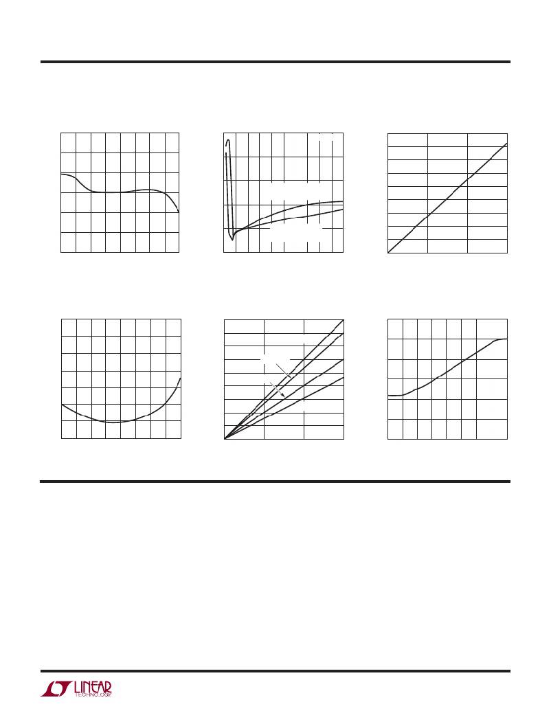
�TYPICAL� PERFORMANCE� CHARACTERISTICS�
�Minimum� Input� Voltage� with� 5V�
�Switching� Frequency�
�Output�
�BOOST� Pin� Current�
�230�
�7.5�
�T� A� = 25°C�
�45�
�T� A� =� 25°C�
�40�
�220�
�210�
�7.0�
�35�
�30�
�200�
�190�
�180�
�6.5�
�6.0�
�5.5�
�MINIMUM� INPUT�
�VOLTAGE� TO� START�
�MINIMUM� INPUT�
�VOLTAGE� TO� RUN�
�25�
�20�
�15�
�10�
�5�
�170�
�–50� –25�
�0�
�25�
�50�
�75�
�100� 125�
�150�
�5.0�
�0�
�0.1� 0.2� 0.3� 0.4� 0.5� 0.6� 0.7� 0.8� 0.9�
�1�
�0�
�0�
�0.5� 1�
�1.5�
�2.1�
�JUNCTION� TEMPERATURE� (°C)�
�V� C� Pin� Shutdown� Threshold�
�1766� G10�
�450�
�LOAD� CURRENT� (A)�
�Switch� Voltage� Drop�
�1766� G11�
�600�
�SWITCH� CURRENT� (A)�
�Switch� Minimum� On-Time�
�vs� Temperature�
�1766� G12�
�1.9�
�400�
�T� J� =� 150°C�
�500�
�350�
�1.7�
�1.5�
�1.3�
�1.1�
�0.9�
�300�
�250�
�200�
�150�
�100�
�50�
�T� J� =� 125°C�
�T� J� =� 25°C�
�T� J� =� –40°C�
�400�
�300�
�200�
�100�
�0.7�
�–50� –25�
�0�
�25�
�50�
�75�
�100� 125� 150�
�0�
�0�
�0.5� 1�
�1.5�
�0�
�–50� –25�
�0�
�25�
�50�
�75�
�100� 125� 150�
�JUNCTION� TEMPERATURE� (°C)�
�PIN� FUNCTIONS�
�1766� G13�
�SWITCH� CURRENT� (A)�
�1766� G14�
�JUNCTION� TEMPERATURE� (°C)�
�1766� G15�
�GND� (Pins� 1,� 8,� 9,� 16,� 17):� The� GND� pin� connections� act�
�as� the� reference� for� the� regulated� output,� so� load� regula-�
�tion� will� suffer� if� the� ground� end� of� the� load� is� not� at� the�
�same� voltage� as� the� GND� pins� of� the� IC.� This� condition� will�
�occur� when� load� current� or� other� currents� ?ow� through�
�metal� paths� between� the� GND� pins� and� the� load� ground.�
�Keep� the� paths� between� the� GND� pins� and� the� load� ground�
�short� and� use� a� ground� plane� when� possible.� The� GND�
�pin� also� acts� as� a� heat� sink� and� should� be� soldered� to� a�
�large� copper� plane� to� reduce� thermal� resistance.� For� the�
�copper� ground� plane� underneath� the� device.� (See� Applica-�
�tions� Information—Layout� Considerations.)�
�SW� (Pin� 2):� The� switch� pin� is� the� emitter� of� the� on-chip�
�power� NPN� switch.� This� pin� is� driven� up� to� the� input� pin�
�voltage� during� switch� on-time.� Inductor� current� drives� the�
�switch� pin� negative� during� switch� off-time.� Negative� volt-�
�age� is� clamped� with� the� external� catch� diode.� Maximum�
�negative� switch� voltage� allowed� is� –� 0.8V.�
�NC� (Pins� 3,� 5,� 7,� 13):� No� Connection.�
�FE� package,� the� exposed� pad� should� be� soldered� to� the�
�1766fc�
�7�
�相关PDF资料 |
PDF描述 |
|---|---|
| HM73-40R40LFTR13 | INDUCTOR 0.40UH LOW PRO SHLD SMD |
| HM70-302R0LFTR13 | HIGH PWR LOW PROFILE INDUCTORS |
| LT1766EFE-5#TR | IC REG BUCK 5V 1.5A 16TSSOP |
| MAX6795TPTD0+ | IC REG LIN W/SPR VSR 20-TQFN |
| MAX6795TPZD0+ | IC REG LIN W/SPR VSR 20-TQFN |
相关代理商/技术参数 |
参数描述 |
|---|---|
| LT1766EFEPBF | 制造商:Linear Technology 功能描述:Sw. Regulator Step-Dn 1.5A 200kHz TSSOP |
| LT1766EFE-PBF | 制造商:LINER 制造商全称:Linear Technology 功能描述:5.5V to 60V 1.5A, 200kHz Step-Down Switching Regulator |
| LT1766EFE-TR | 制造商:LINER 制造商全称:Linear Technology 功能描述:5.5V to 60V 1.5A, 200kHz Step-Down Switching Regulator |
| LT1766EFE-TRPBF | 制造商:LINER 制造商全称:Linear Technology 功能描述:5.5V to 60V 1.5A, 200kHz Step-Down Switching Regulator |
| LT1766EGN | 功能描述:IC REG BUCK ADJ 1.5A 16SSOP RoHS:否 类别:集成电路 (IC) >> PMIC - 稳压器 - DC DC 开关稳压器 系列:- 标准包装:2,500 系列:- 类型:降压(降压) 输出类型:固定 输出数:1 输出电压:1.2V,1.5V,1.8V,2.5V 输入电压:2.7 V ~ 20 V PWM 型:- 频率 - 开关:- 电流 - 输出:50mA 同步整流器:是 工作温度:-40°C ~ 125°C 安装类型:表面贴装 封装/外壳:10-TFSOP,10-MSOP(0.118",3.00mm 宽)裸露焊盘 包装:带卷 (TR) 供应商设备封装:10-MSOP 裸露焊盘 |
发布紧急采购,3分钟左右您将得到回复。