参数资料
| 型号: | LT1766HFE#TRPBF |
| 厂商: | Linear Technology |
| 文件页数: | 5/30页 |
| 文件大小: | 0K |
| 描述: | IC REG BUCK ADJ 1.5A 16TSSOP |
| 标准包装: | 2,500 |
| 类型: | 降压(降压) |
| 输出类型: | 可调式 |
| 输出数: | 1 |
| 输出电压: | 1.2 V ~ 54 V |
| 输入电压: | 5.5 V ~ 60 V |
| PWM 型: | 电流模式 |
| 频率 - 开关: | 200kHz |
| 电流 - 输出: | 1.5A |
| 同步整流器: | 无 |
| 工作温度: | -40°C ~ 140°C |
| 安装类型: | 表面贴装 |
| 封装/外壳: | 16-TSSOP(0.173",4.40mm)裸露焊盘 |
| 包装: | 带卷 (TR) |
| 供应商设备封装: | 16-TSSOP-EP |
第1页第2页第3页第4页当前第5页第6页第7页第8页第9页第10页第11页第12页第13页第14页第15页第16页第17页第18页第19页第20页第21页第22页第23页第24页第25页第26页第27页第28页第29页第30页
�� �
�
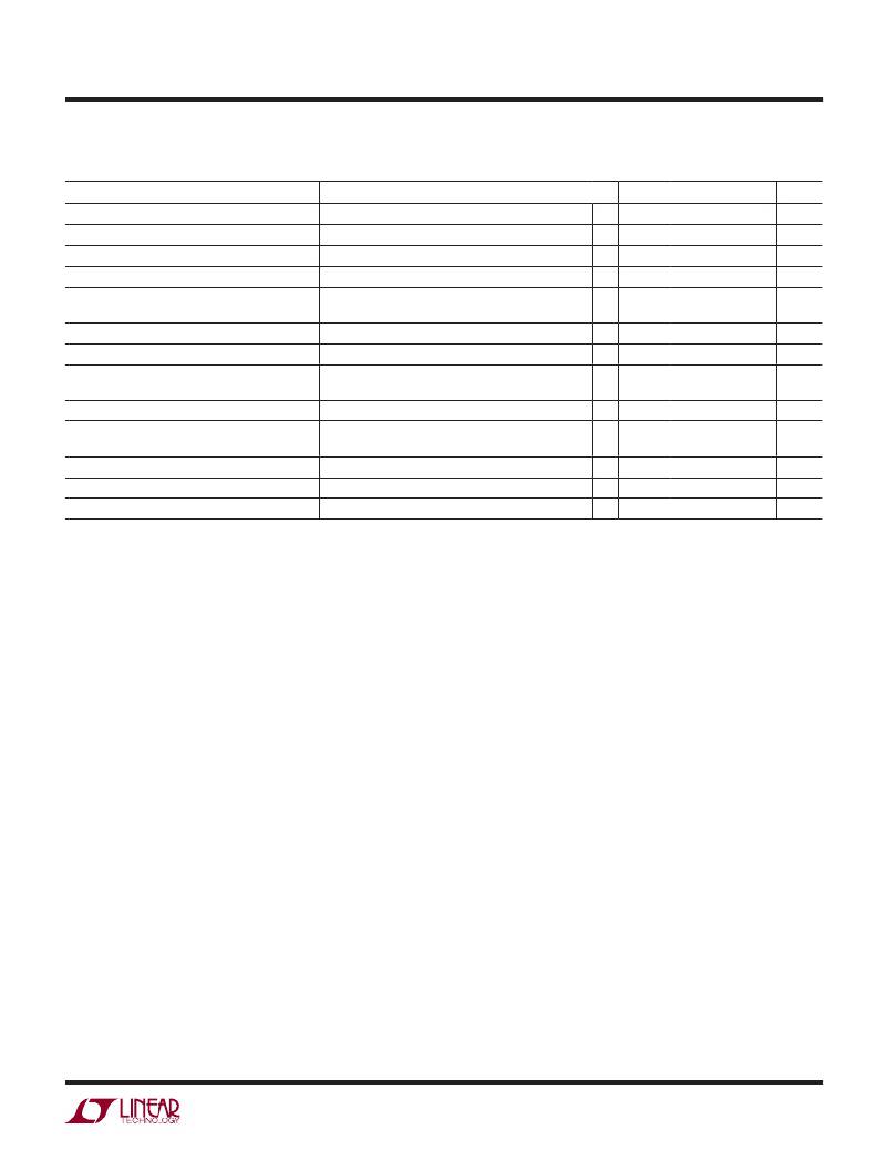
�LT1766/LT1766-5�
�ELECTRICAL� CHARACTERISTICS�
�(LT1766H� Grade)�
�The� l� denotes� speci?cations� which� apply� over� the� full� operating� temperature� range,� otherwise� speci?cations� are� at� T� J� =� 25°C.�
�V� IN� =� 15V,� V� C� =� 1.5V,� SHDN� =� 1V,� BOOST� open� circuit,� SW� open� circuit,� unless� otherwise� noted.�
�PARAMETER�
�f� SW� Line� Regulation�
�f� SW� Frequency� Shifting� Threshold�
�Minimum� Input� Voltage�
�Minimum� Boost� Voltage�
�Boost� Current� (Note� 5)�
�Input� Supply� Current� (I� VIN� )�
�Bias� Supply� Current� (I� BIAS� )�
�Shutdown� Supply� Current�
�CONDITIONS�
�5.5V� ≤� V� IN� ≤� 60V�
�Df� =� 10kHz�
�(Note� 3)�
�(Note� 4)� I� SW� ≤� 0.75A�
�Boost� =� V� IN� +� 5V,� I� SW� =� 0.5A�
�Boost� =� V� IN� +� 5V,� I� SW� =� 0.75A�
�(Note� 6)� V� BIAS� =� 5V�
�(Note� 6)� V� BIAS� =� 5V�
�SHDN� =� 0V,� V� IN� ≤� 60V,� SW� =� 0V,� V� C� Open�
�l�
�l�
�l�
�l�
�l�
�l�
�MIN�
�TYP�
�0.05�
�0.8�
�4.6�
�1.8�
�12�
�45�
�1.4�
�2.9�
�25�
�MAX�
�0.15�
�5.5�
�3�
�40�
�100�
�2.2�
�4.2�
�120�
�500�
�UNITS�
�%/V�
�V�
�V�
�V�
�mA�
�mA�
�mA�
�mA�
�μA�
�μA�
�Lockout� Threshold�
�Shutdown� Thresholds�
�Minimum� SYNC� Amplitude�
�V� C� Open�
�V� C� Open,� Shutting� Down�
�V� C� Open,� Starting� Up�
�l�
�l�
�l�
�l�
�2.3�
�0.15�
�0.25�
�2.42�
�0.37�
�0.45�
�1.5�
�2.68�
�0.9�
�0.9�
�2.2�
�V�
�V�
�V�
�V�
�SYNC� Frequency� Range�
�SYNC� Input� Resistance�
�228�
�20�
�700�
�kHz�
�k�
�Note� 1:� Stresses� beyond� those� listed� under� Absolute� Maximum� Ratings�
�may� cause� permanent� damage� to� the� device.� Exposure� to� any� Absolute�
�Maximum� Rating� condition� for� extended� periods� may� affect� device�
�reliability� and� lifetime.�
�Note� 2:� Gain� is� measured� with� a� V� C� swing� equal� to� 200mV� above� the� low�
�clamp� level� to� 200mV� below� the� upper� clamp� level.�
�Note� 3:� Minimum� input� voltage� is� not� measured� directly,� but� is� guaranteed�
�by� other� tests.� It� is� de?ned� as� the� voltage� where� internal� bias� lines� are� still�
�regulated� so� that� the� reference� voltage� and� oscillator� remain� constant.�
�Actual� minimum� input� voltage� to� maintain� a� regulated� output� will� depend�
�upon� output� voltage� and� load� current.� See� Applications� Information.�
�Note� 4:� This� is� the� minimum� voltage� across� the� boost� capacitor� needed� to�
�guarantee� full� saturation� of� the� internal� power� switch.�
�Note� 5:� Boost� current� is� the� current� ?owing� into� the� BOOST� pin� with� the�
�pin� held� 5V� above� input� voltage.� It� ?ows� only� during� switch� on� time.�
�Note� 6:� Input� supply� current� is� the� quiescent� current� drawn� by� the� input�
�pin� when� the� BIAS� pin� is� held� at� 5V� with� switching� disabled.� Bias� supply�
�current� is� the� current� drawn� by� the� BIAS� pin� when� the� BIAS� pin� is� held�
�at� 5V.� Total� input� referred� supply� current� is� calculated� by� summing� input�
�supply� current� (I� VIN� )� with� a� fraction� of� bias� supply� current� (I� BIAS� ):�
�I� TOTAL� =� I� VIN� +� (I� BIAS� )(V� OUT� /V� IN� )�
�with� V� IN� =� 15V,� V� OUT� =� 5V,� I� VIN� =� 1.4mA,� I� BIAS� =� 2.9mA,� I� TOTAL� =� 2.4mA.�
�Note� 7:� Switch� on-resistance� is� calculated� by� dividing� V� IN� to� SW� voltage�
�by� the� forced� current.� See� Typical� Performance� Characteristics� for� the�
�graph� of� switch� voltage� at� other� currents.�
�Note� 8:� The� LT1766EGN,� LT1766EGN-5,� LT1766EFE� and� LT1766EFE-5�
�are� guaranteed� to� meet� performance� speci?cations� from� 0°C� to� 125°C�
�junction� temperature.� Speci?cations� over� the� –40°C� to� 125°C� operating�
�junction� temperature� range� are� assured� by� design,� characterization� and�
�correlation� with� statistical� process� controls.� The� LT1766IGN,� LT1766IGN-5,�
�LT1766IFE� and� LT1766IFE-5� are� guaranteed� over� the� full� –40°C� to� 125°C�
�operating� junction� temperature� range.� The� LT1766HGN� and� LT1766HFE� are�
�guaranteed� over� the� full� –40°C� to� 140°C� operating� junction� temperature�
�range.�
�Note� 9:� Transconductance� and� voltage� gain� refer� to� the� internal� ampli?er�
�exclusive� of� the� voltage� divider.� To� calculate� gain� and� transconductance,�
�refer� to� the� SENSE� pin� on� ?xed� voltage� parts.� Divide� the� values� shown� by�
�the� ratio� V� OUT� /1.219.�
�Note� 10:� This� IC� includes� overtemperature� protection� that� is� intended�
�to� protect� the� device� during� momentary� overload� conditions.� Junction�
�temperature� will� exceed� 140°C� when� overtemperature� protection� is� active.�
�Continuous� operation� above� the� speci?ed� maximum� operating� junction�
�temperature� may� impair� device� reliability.�
�Note� 11:� High� junction� temperatures� degrade� operating� lifetimes.�
�Operating� lifetime� at� junction� temperatures� between� 125°C� and� 140°C� is�
�derated� to� 1000� hours.�
�1766fc�
�5�
�相关PDF资料 |
PDF描述 |
|---|---|
| LT1767EMS8-2.5 | IC REG BUCK 2.5V 1.5A 8MSOP |
| LT1768IGN#TR | IC CTRLR CCFL SGL/MULT HP 16SSOP |
| LT1769CGN | IC BATT CHARGER CONST I/V 28SSOP |
| LT1776IS8#TR | IC REG BUCK ADJ 0.7A 8SOIC |
| LT1777IS#TRPBF | IC REG BUCK ADJ 0.7A 16SOIC |
相关代理商/技术参数 |
参数描述 |
|---|---|
| LT1766IFE | 功能描述:IC REG BUCK ADJ 1.5A 16TSSOP RoHS:否 类别:集成电路 (IC) >> PMIC - 稳压器 - DC DC 开关稳压器 系列:- 设计资源:Design Support Tool 标准包装:1 系列:- 类型:升压(升压) 输出类型:固定 输出数:1 输出电压:3V 输入电压:0.75 V ~ 2 V PWM 型:- 频率 - 开关:- 电流 - 输出:100mA 同步整流器:是 工作温度:-40°C ~ 85°C 安装类型:表面贴装 封装/外壳:SOT-23-5 细型,TSOT-23-5 包装:剪切带 (CT) 供应商设备封装:TSOT-23-5 其它名称:AS1323-BTTT-30CT |
| LT1766IFE#PBF | 功能描述:IC REG BUCK ADJ 1.5A 16TSSOP RoHS:是 类别:集成电路 (IC) >> PMIC - 稳压器 - DC DC 开关稳压器 系列:- 产品培训模块:MIC23xxx HyperLight Load™ Regulators 标准包装:5,000 系列:HyperLight Load® 类型:降压(降压) 输出类型:固定 输出数:1 输出电压:1.8V 输入电压:2.7 V ~ 5.5 V PWM 型:混合物 频率 - 开关:4MHz 电流 - 输出:2A 同步整流器:是 工作温度:-40°C ~ 125°C 安装类型:表面贴装 封装/外壳:8-VFDFN 裸露焊盘,8-MLF? 包装:带卷 (TR) 供应商设备封装:8-MLF?(2x2) 产品目录页面:1094 (CN2011-ZH PDF) 其它名称:576-3303-2 |
| LT1766IFE#PBF | 制造商:Linear Technology 功能描述:IC STEP-DOWN REGULATOR 16-TSSOP |
| LT1766IFE#TR | 功能描述:IC REG BUCK ADJ 1.5A 16TSSOP RoHS:否 类别:集成电路 (IC) >> PMIC - 稳压器 - DC DC 开关稳压器 系列:- 设计资源:Design Support Tool 标准包装:1 系列:- 类型:升压(升压) 输出类型:固定 输出数:1 输出电压:3V 输入电压:0.75 V ~ 2 V PWM 型:- 频率 - 开关:- 电流 - 输出:100mA 同步整流器:是 工作温度:-40°C ~ 85°C 安装类型:表面贴装 封装/外壳:SOT-23-5 细型,TSOT-23-5 包装:剪切带 (CT) 供应商设备封装:TSOT-23-5 其它名称:AS1323-BTTT-30CT |
| LT1766IFE#TRPBF | 功能描述:IC REG BUCK ADJ 1.5A 16TSSOP RoHS:是 类别:集成电路 (IC) >> PMIC - 稳压器 - DC DC 开关稳压器 系列:- 设计资源:Design Support Tool 标准包装:1 系列:- 类型:升压(升压) 输出类型:固定 输出数:1 输出电压:3V 输入电压:0.75 V ~ 2 V PWM 型:- 频率 - 开关:- 电流 - 输出:100mA 同步整流器:是 工作温度:-40°C ~ 85°C 安装类型:表面贴装 封装/外壳:SOT-23-5 细型,TSOT-23-5 包装:剪切带 (CT) 供应商设备封装:TSOT-23-5 其它名称:AS1323-BTTT-30CT |
发布紧急采购,3分钟左右您将得到回复。