参数资料
| 型号: | LT1768IGN#TR |
| 厂商: | Linear Technology |
| 文件页数: | 13/20页 |
| 文件大小: | 0K |
| 描述: | IC CTRLR CCFL SGL/MULT HP 16SSOP |
| 标准包装: | 2,500 |
| 类型: | CCFL 控制器 |
| 频率: | 300 ~ 410 kHz |
| 电流 - 电源: | 7mA |
| 电流 - 输出: | 1.5A |
| 电源电压: | 9 V ~ 24 V |
| 工作温度: | -40°C ~ 125°C |
| 封装/外壳: | 16-SSOP(0.154",3.90mm 宽) |
| 供应商设备封装: | 16-SSOP |
| 包装: | 带卷 (TR) |
�� �
�
�LT1768�
�APPLICATIO� N� S� I� N� FOR� M� ATIO� N�
�voltage� and� DIO� lines� can� cause� enough� current� flow� to�
�fool� the� open� lamp� detection.� In� situations� where� coupling�
�can’t� be� avoided,� resistors� can� be� added� from� the� DIO� pins�
�to� ground� to� increase� the� open� lamp� threshold.� When�
�resistors� from� the� DIO� pins� to� ground� are� added,� the�
�values� for� R� RMAX� and� R� RMIN� may� need� to� be� increased�
�from� their� nominal� values� to� compensate� for� the� additional�
�current.�
�For� single� lamp� operation,� the� lowside� of� the� lamp� should�
�be� connected� to� both� DIO� pins,� and� the� values� of� R� RMAX�
�and� R� RMIN� increased� to� two� times� the� values� that� would� be�
�used� in� a� dual� lamp� configuration.� In� single� lamp� mode� all�
�fault� detection� will� operate� as� in� the� dual� lamp� configura-�
�tion,� but� the� open� lamp� threshold� will� double.� If� the�
�increase� in� the� open� lamp� threshold� is� not� acceptable,� a�
�positive� offset� current� can� be� added� to� reduce� the� open�
�lamp� threshold� by� placing� a� resistor� between� the� REF� and�
�DIO� pins� (a� 33k� resistor� will� reduce� the� open� lamp� thresh-�
�old� by� approximately� 100� μ� A� ((V� REF� –� V� DIO+� )/33k).� When�
�an� offset� current� is� added,� the� values� for� R� RMAX� and� R� RMIN�
�may� need� to� be� increased� from� their� nominal� values� to�
�compensate� for� the� offset� current.�
�VC� Compensation�
�As� previously� mentioned� a� single� capacitor� on� the� VC� pin�
�combines� the� error� signal� conversion,� lamp� current� aver-�
�aging� and� frequency� compensation.� Careful� consideration�
�should� be� given� to� the� value� of� capacitance� used.� A� large�
�value� (1� μ� F)� will� give� excellent� stability� at� high� lamp� cur-�
�rents� but� will� result� in� degraded� line� regulation� in� PWM�
�mode.� On� the� other� hand� ,� a� small� value� (10nF)� will� give�
�excellent� PWM� response� but� might� result� in� overshoot� and�
�poor� load� regulation.� The� value� chosen� will� depend� on� the�
�maximum� load� current� and� dimming� range.� After� these�
�parameters� are� decided� upon,� the� value� of� the� VC� capacitor�
�should� be� increased� until� the� line� regulation� becomes�
�start� of� every� oscillator� cycle.� The� GATE� is� driven� back� low�
�when� the� current� reaches� a� threshold� level� proportional� to�
�the� voltage� on� the� VC� pin.� The� GATE� then� remains� low� until�
�the� start� of� the� next� oscillator� cycle.� The� peak� current� is�
�thus� proportional� to� the� VC� voltage� and� controlled� on� a�
�cycle� by� cycle� basis.� The� peak� switch� current� is� normally�
�sensed� by� placing� a� sense� resistor� in� the� source� lead� of� the�
�output� MOSFET.� This� resistor� converts� the� switch� current�
�to� a� voltage� that� can� be� compared� to� a� fraction� of� the� VC�
�voltage� [(V� VC� –� V� DIODE� )/30]� .� For� normal� conditions� and� a�
�GATE� duty� cycle� below� 50%,� the� switch� current� limit� will�
�correspond� to� I� PK� =� 0.1/R� SENSE� .� For� GATE� duty� cycles�
�above� 50%� the� switch� current� limit� will� be� reduced�
�to� approximately� 90mV� at� 80%� duty� cycle� to� avoid�
�subharmonic� oscillations� associated� with� current� mode�
�controllers.�
�When� the� lamp� current� is� programmed� to� PWM� mode,� the�
�VC� pin� will� slew� between� voltages� that� represent� the�
�minimum� and� maximum� PWM� lamp� currents.� The� slew�
�time� affects� the� line� regulation� at� low� duty� cycle,� and�
�should� be� kept� low� by� making� the� sense� resistor� as� small�
�as� possible.� The� lowest� value� of� sense� resistor� is� deter-�
�mined� by� switching� transients� and� other� noise� due� to�
�layout� configurations.� A� good� rule� of� thumb� is� to� set� the�
�sense� resistor� so� that� the� voltage� on� the� VC� pin� equals�
�2.5V� when� the� PWM� current� is� in� maximum� mode� (V� PROG�
�=� V� PWM� ).� Typical� values� of� the� sense� resistor� run� in� the�
�25m� ?� to� 50m� ?� range� for� large� displays,� and� can� be�
�implemented� with� a� copper� trace� on� the� PCB.�
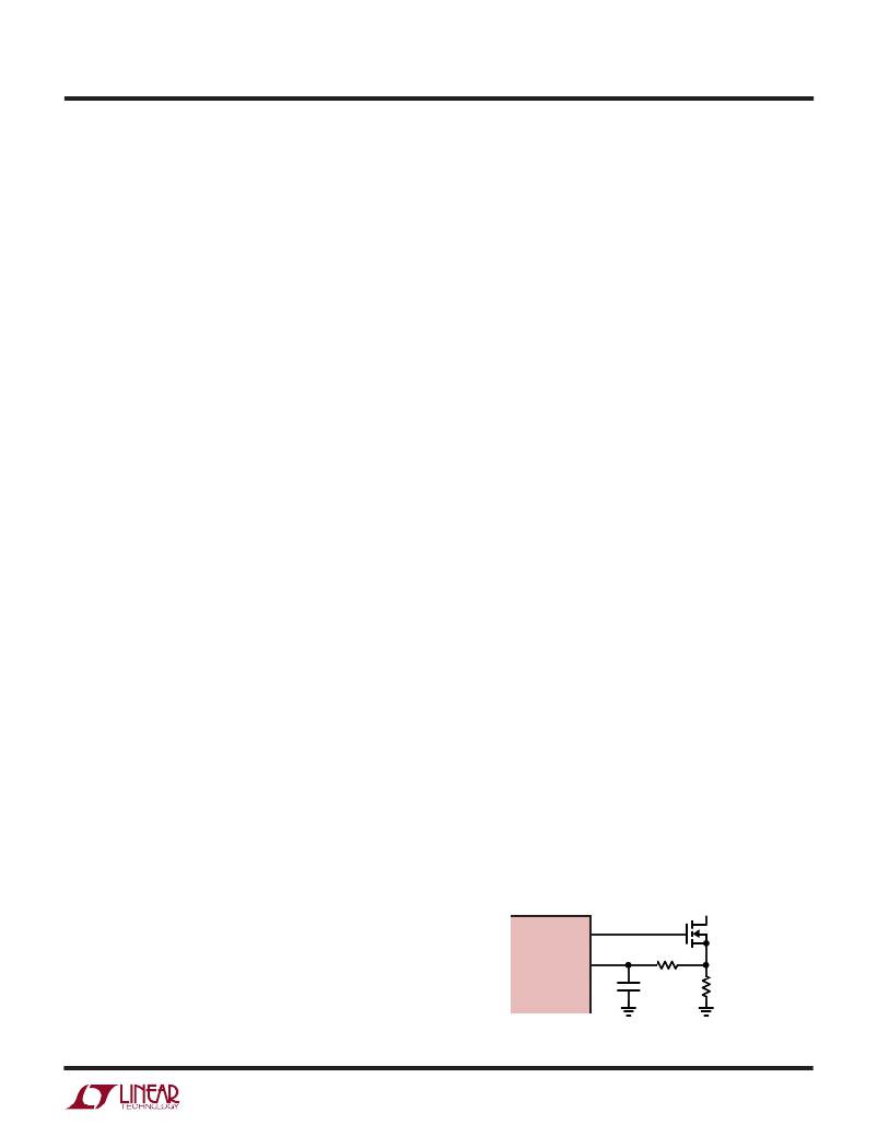
�Since� the� maximum� threshold� at� the� SENSE� pin� is� only�
�100mV,� switching� transients� and� other� noise� can� prema-�
�turely� trip� the� comparator.� The� LT1768� has� a� blanking�
�period� of� 100ns� which� prohibits� premature� switch� turn�
�off,� but� further� filtering� the� sense� resistor� voltage� is�
�recommended.� A� simple� RC� filter� is� adequate� for� most�
�applications.� (Figure� 5.)�
�unacceptable.� A� typical� value� for� the� VC� capacitor� is�
�0.033� μ� F.� For� further� information� on� compensation� please�
�refer� to� the� references� or� consult� the� factory.�
�LT1768�
�GATE�
�100� ?�
�SENSE�
�Current� Sense� Comparator�
�2.2nF�
�0.025m� ?�
�The� LT1768� is� a� current� mode� PWM� controller.� Under�
�normal� operating� conditions� the� GATE� is� driven� high� at� the�
�Figure� 5.� Sense� Pin� Filter�
�1768� ?F05�
�13�
�相关PDF资料 |
PDF描述 |
|---|---|
| LT1769CGN | IC BATT CHARGER CONST I/V 28SSOP |
| LT1776IS8#TR | IC REG BUCK ADJ 0.7A 8SOIC |
| LT1777IS#TRPBF | IC REG BUCK ADJ 0.7A 16SOIC |
| LT1786FCS#TR | IC REG SW CCFL SMBUS PROG 16SOIC |
| LT1912EMSE#TRPBF | IC REG BUCK ADJ 2A 10MSOP |
相关代理商/技术参数 |
参数描述 |
|---|---|
| LT1769 | 制造商:LINER 制造商全称:Linear Technology 功能描述:4A, High Efficiency, Standalone Li Battery Charger |
| LT1769CFE | 功能描述:IC BATT CHRGR CNSTNT I/V 20TSSOP RoHS:否 类别:集成电路 (IC) >> PMIC - 电池管理 系列:- 产品培训模块:Lead (SnPb) Finish for COTS Obsolescence Mitigation Program 标准包装:2,500 系列:- 功能:电池监控器 电池化学:碱性,锂离子,镍镉,镍金属氢化物 电源电压:1 V ~ 5.5 V 工作温度:-40°C ~ 85°C 安装类型:表面贴装 封装/外壳:SOT-23-6 供应商设备封装:SOT-6 包装:带卷 (TR) |
| LT1769CFE#PBF | 功能描述:IC BATT CHRGR CNSTNT I/V 20TSSOP RoHS:是 类别:集成电路 (IC) >> PMIC - 电池管理 系列:- 产品培训模块:Lead (SnPb) Finish for COTS Obsolescence Mitigation Program 标准包装:2,500 系列:- 功能:电池监控器 电池化学:碱性,锂离子,镍镉,镍金属氢化物 电源电压:1 V ~ 5.5 V 工作温度:-40°C ~ 85°C 安装类型:表面贴装 封装/外壳:SOT-23-6 供应商设备封装:SOT-6 包装:带卷 (TR) |
| LT1769CFE#TR | 功能描述:IC BATT CHRGR CNSTNT I/V 20TSSOP RoHS:否 类别:集成电路 (IC) >> PMIC - 电池管理 系列:- 产品培训模块:Lead (SnPb) Finish for COTS Obsolescence Mitigation Program 标准包装:2,500 系列:- 功能:电池监控器 电池化学:碱性,锂离子,镍镉,镍金属氢化物 电源电压:1 V ~ 5.5 V 工作温度:-40°C ~ 85°C 安装类型:表面贴装 封装/外壳:SOT-23-6 供应商设备封装:SOT-6 包装:带卷 (TR) |
| LT1769CFE#TRPBF | 功能描述:IC BATT CHRGR CNSTNT I/V 20TSSOP RoHS:是 类别:集成电路 (IC) >> PMIC - 电池管理 系列:- 产品培训模块:Lead (SnPb) Finish for COTS Obsolescence Mitigation Program 标准包装:2,500 系列:- 功能:电池监控器 电池化学:碱性,锂离子,镍镉,镍金属氢化物 电源电压:1 V ~ 5.5 V 工作温度:-40°C ~ 85°C 安装类型:表面贴装 封装/外壳:SOT-23-6 供应商设备封装:SOT-6 包装:带卷 (TR) |
发布紧急采购,3分钟左右您将得到回复。