参数资料
| 型号: | LT1768IGN#TR |
| 厂商: | Linear Technology |
| 文件页数: | 14/20页 |
| 文件大小: | 0K |
| 描述: | IC CTRLR CCFL SGL/MULT HP 16SSOP |
| 标准包装: | 2,500 |
| 类型: | CCFL 控制器 |
| 频率: | 300 ~ 410 kHz |
| 电流 - 电源: | 7mA |
| 电流 - 输出: | 1.5A |
| 电源电压: | 9 V ~ 24 V |
| 工作温度: | -40°C ~ 125°C |
| 封装/外壳: | 16-SSOP(0.154",3.90mm 宽) |
| 供应商设备封装: | 16-SSOP |
| 包装: | 带卷 (TR) |
�� �
�
�LT1768�
�APPLICATIO� N� S� I� N� FOR� M� ATIO� N�
�GATE�
�The� LT1768� has� a� single� high� current� totem� pole� output�
�stage.� This� output� stage� is� capable� of� driving� up� to� ±� 1.5A�
�of� output� current.� Cross-conduction� current� spikes� in� the�
�totem� pole� output� have� been� eliminated.� The� GATE� pin� is�
�intended� to� drive� an� N-channel� MOSFET� switch.� Rise� and�
�fall� times� are� typically� 50ns� with� a� 3000pF� load.� A� clamp�
�is� built� into� the� device� to� prevent� the� GATE� pin� from� rising�
�above� 13V� in� order� to� protect� the� gate� of� the� MOSFET�
�switch.�
�The� GATE� pin� connects� directly� to� the� emitter� of� the� upper�
�NPN� drive� transistor� and� the� collector� of� the� lower� NPN�
�drive� transistor� in� the� totem� pole.� The� collector� of� the� lower�
�transistor,� which� is� N-type� silicon,� forms� a� P-N� junction�
�with� the� substrate� of� the� device.� This� junction� is� reversed�
�biased� during� normal� operation.�
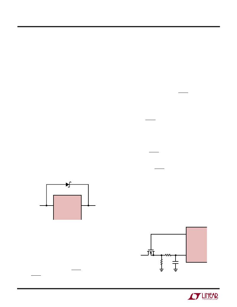
�In� some� applications� the� parasitic� LC� of� the� external�
�MOSFET� gate� can� ring� and� pull� the� GATE� pin� below�
�ground.� If� the� GATE� pin� is� pulled� negative� by� more� than� a�
�diode� drop� the� parasitic� diode� formed� by� the� collector� of�
�the� GATE� NPN� and� the� substrate� will� turn� on.� This� can�
�cause� erratic� operation� of� the� device.� In� these� cases� a�
�Schottky� clamp� diode� is� recommended� from� the� GATE� pin�
�to� ground.� (Figure� 6.)�
�BAT� 85�
�up� current� source.� The� LT1768� thermal� shutdown� tem-�
�perature� is� set� at� 160� °� C.� A� buffered� version� of� the� internal�
�5V� is� present� at� the� V� REF� pin� and� is� capable� of� supplying� up�
�to� 10mA� of� current.� Note� that� using� any� substantial�
�amount� of� current� from� the� V� REF� pin� will� increase� power�
�dissipation� in� the� device,� which� will� reduce� the� useful�
�operating� ambient� temperature� range.�
�Supply� and� Input� Voltage� Sequencing�
�For� most� applications,� where� the� SHDN� pin� is� left� floating,�
�and� the� voltages� on� the� PWM� and� PROG� pins� are� derived�
�from� the� V� REF� pin,� the� LT1768� will� power-up� and� power-�
�down� correctly� when� the� voltage� to� the� V� IN� pin� is� applied�
�and� removed.� In� applications� where� the� voltage� inputs� for�
�the� V� IN� pin,� SHDN� pin,� PWM� pin,� and� the� PROG� pin�
�originate� from� different� sources� (power� supply,� micropro-�
�cessors� etc.),� care� must� be� taken� during� power� up/down�
�sequences.� For� proper� operation� during� the� power-up�
�sequence,� the� voltage� on� the� following� pins� must� be� taken�
�from� zero� to� their� appropriate� values� in� the� following�
�order;� V� IN� pin,� SHDN� pin,� PWM� pin� and� PROG� pin.� For�
�proper� operation� during� the� power-down� sequence,� the�
�order� must� be� reversed.� For� example,� in� the� circuit� of�
�Figure� 1� where� the� SHDN� pin� is� left� floating,� and� the� PWM�
�pin� voltage� is� derived� from� a� resistor� divider� to� the� V� REF�
�pin,� the� proper� power-up� sequence� would� be� to� take� the�
�V� IN� pin� from� zero� to� its� value� then� apply� either� a� voltage� or�
�PWM� signal� to� the� PROG� pin.� The� power-down� sequence�
�PGND�
�LT1768�
�GATE�
�for� the� circuit� in� Figure� 1� would� be� to� take� the� PROG� pin�
�voltage� to� zero,� then� take� the� V� IN� pin� voltage� to� zero.If� the�
�PROG� voltage� in� the� circuit� of� Figure� 1� is� present� before� the�
�V� IN� supply� voltage,� proper� power� supply� sequecing� can� be�
�1768� ?� G06�
�Figure� 6.� Schottky� Gate� Clamp�
�Reference�
�The� internal� reference� of� the� LT1768� is� a� trimmed� bandgap�
�reference.� The� reference� is� used� to� power� the� majority� of�
�achieved� by� implementing� the� circuit� shown� in� Figure� 7.�
�V� IN�
�LT1768�
�the� LT1768� internal� circuitry.� The� reference� is� inactive� if�
�0� TO� 5V�
�49.9k�
�the� LT1768� is� in� undervoltage� lockout,� shutdown� mode,� or�
�thermal� shutdown.� The� undervoltage� lockout� is� active�
�OR�
�1kHz� PWM�
�VN2222LL�
�10k�
�10� μ� F�
�PROG�
�when� V� IN� is� below� 7.9V� and� the� LT1768� is� in� shutdown�
�mode� when� the� voltage� on� the� SHDN� pin� is� pulled� below�
�1V.� The� SHDN� pin� has� 200mV� of� hysteresis� and� a� 7� μ� A� pull-�
�14�
�1768� F07�
�Figure� 7.� Circuit� Insures� Proper� Supply� Sequencing� When�
�Dimming� Voltage� Exists� Before� Main� Power� Supply�
�相关PDF资料 |
PDF描述 |
|---|---|
| LT1769CGN | IC BATT CHARGER CONST I/V 28SSOP |
| LT1776IS8#TR | IC REG BUCK ADJ 0.7A 8SOIC |
| LT1777IS#TRPBF | IC REG BUCK ADJ 0.7A 16SOIC |
| LT1786FCS#TR | IC REG SW CCFL SMBUS PROG 16SOIC |
| LT1912EMSE#TRPBF | IC REG BUCK ADJ 2A 10MSOP |
相关代理商/技术参数 |
参数描述 |
|---|---|
| LT1769 | 制造商:LINER 制造商全称:Linear Technology 功能描述:4A, High Efficiency, Standalone Li Battery Charger |
| LT1769CFE | 功能描述:IC BATT CHRGR CNSTNT I/V 20TSSOP RoHS:否 类别:集成电路 (IC) >> PMIC - 电池管理 系列:- 产品培训模块:Lead (SnPb) Finish for COTS Obsolescence Mitigation Program 标准包装:2,500 系列:- 功能:电池监控器 电池化学:碱性,锂离子,镍镉,镍金属氢化物 电源电压:1 V ~ 5.5 V 工作温度:-40°C ~ 85°C 安装类型:表面贴装 封装/外壳:SOT-23-6 供应商设备封装:SOT-6 包装:带卷 (TR) |
| LT1769CFE#PBF | 功能描述:IC BATT CHRGR CNSTNT I/V 20TSSOP RoHS:是 类别:集成电路 (IC) >> PMIC - 电池管理 系列:- 产品培训模块:Lead (SnPb) Finish for COTS Obsolescence Mitigation Program 标准包装:2,500 系列:- 功能:电池监控器 电池化学:碱性,锂离子,镍镉,镍金属氢化物 电源电压:1 V ~ 5.5 V 工作温度:-40°C ~ 85°C 安装类型:表面贴装 封装/外壳:SOT-23-6 供应商设备封装:SOT-6 包装:带卷 (TR) |
| LT1769CFE#TR | 功能描述:IC BATT CHRGR CNSTNT I/V 20TSSOP RoHS:否 类别:集成电路 (IC) >> PMIC - 电池管理 系列:- 产品培训模块:Lead (SnPb) Finish for COTS Obsolescence Mitigation Program 标准包装:2,500 系列:- 功能:电池监控器 电池化学:碱性,锂离子,镍镉,镍金属氢化物 电源电压:1 V ~ 5.5 V 工作温度:-40°C ~ 85°C 安装类型:表面贴装 封装/外壳:SOT-23-6 供应商设备封装:SOT-6 包装:带卷 (TR) |
| LT1769CFE#TRPBF | 功能描述:IC BATT CHRGR CNSTNT I/V 20TSSOP RoHS:是 类别:集成电路 (IC) >> PMIC - 电池管理 系列:- 产品培训模块:Lead (SnPb) Finish for COTS Obsolescence Mitigation Program 标准包装:2,500 系列:- 功能:电池监控器 电池化学:碱性,锂离子,镍镉,镍金属氢化物 电源电压:1 V ~ 5.5 V 工作温度:-40°C ~ 85°C 安装类型:表面贴装 封装/外壳:SOT-23-6 供应商设备封装:SOT-6 包装:带卷 (TR) |
发布紧急采购,3分钟左右您将得到回复。