参数资料
| 型号: | LT1936HMS8E#TRPBF |
| 厂商: | Linear Technology |
| 文件页数: | 12/20页 |
| 文件大小: | 0K |
| 描述: | IC REG BUCK ADJ 1.4A 8MSOP |
| 标准包装: | 2,500 |
| 类型: | 降压(降压) |
| 输出类型: | 可调式 |
| 输出数: | 1 |
| 输出电压: | 1.2 V ~ 31.3 V |
| 输入电压: | 3.6 V ~ 36 V |
| PWM 型: | 电流模式 |
| 频率 - 开关: | 500kHz |
| 电流 - 输出: | 1.4A |
| 同步整流器: | 无 |
| 工作温度: | -40°C ~ 150°C |
| 安装类型: | 表面贴装 |
| 封装/外壳: | 8-TSSOP,8-MSOP(0.118",3.00mm 宽)裸露焊盘 |
| 包装: | 带卷 (TR) |
| 供应商设备封装: | 8-MSOP-EP |
�� �
�
�LT1936�
�APPLICATIONS� INFORMATION�
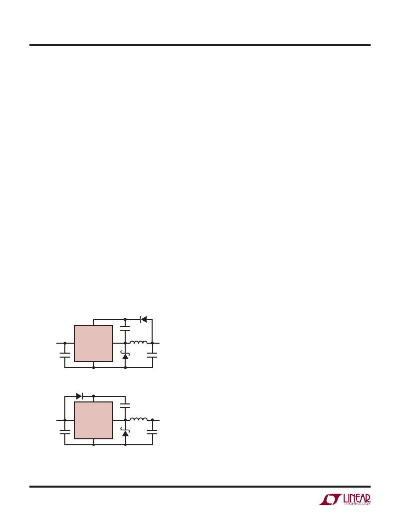
�BOOST� Pin� Considerations�
�Capacitor� C3� and� diode� D2� are� used� to� generate� a� boost�
�voltage� that� is� higher� than� the� input� voltage.� In� most� cases�
�a� 0.22μF� capacitor� and� fast� switching� diode� (such� as� the�
�1N4148� or� 1N914)� will� work� well.� Figure� 3� shows� two�
�ways� to� arrange� the� boost� circuit.� The� BOOST� pin� must�
�be� at� least� 2.3V� above� the� SW� pin� for� best� ef?ciency.� For�
�outputs� of� 3V� and� above,� the� standard� circuit� (Figure� 3a)�
�is� best.� For� outputs� between� 2.8V� and� 3V,� use� a� 0.47μF�
�capacitor� and� a� Schottky� diode.� For� lower� output� voltages�
�the� boost� diode� can� be� tied� to� the� input� (Figure� 3b),� or� to�
�another� supply� greater� than� 2.8V.� The� circuit� in� Figure� 3a� is�
�more� ef?cient� because� the� BOOST� pin� current� comes� from�
�a� lower� voltage.� You� must� also� be� sure� that� the� maximum�
�voltage� rating� of� the� BOOST� pin� is� not� exceeded.�
�A� 2.5V� output� presents� a� special� case.� This� is� a� popular�
�output� voltage,� and� the� advantage� of� connecting� the�
�boost� circuit� to� the� output� is� that� the� circuit� will� accept� a�
�36V� maximum� input� voltage� rather� than� 20V� (due� to� the�
�BOOST� pin� rating).� However,� 2.5V� is� marginally� adequate�
�to� support� the� boosted� drive� stage� at� low� ambient� tem-�
�peratures.� Therefore,� special� care� and� some� restrictions�
�on� operation� are� necessary� when� powering� the� BOOST� pin�
�from� a� 2.5V� output.� Minimize� the� voltage� loss� in� the� boost�
�D2�
�circuit� by� using� a� 1μF� boost� capacitor� and� a� good,� low� drop�
�Schottky� diode� (such� as� the� ON� Semi� MBR0540).� Because�
�the� required� boost� voltage� increases� at� low� temperatures,�
�the� circuit� will� supply� only� 1A� of� output� current� when� the�
�ambient� temperature� is� –45°C,� increasing� to� 1.2A� at� 0°C.�
�Also,� the� minimum� input� voltage� to� start� the� boost� circuit�
�is� higher� at� low� temperature.� See� the� Typical� Applications�
�section� for� a� 2.5V� schematic� and� performance� curves.�
�The� minimum� operating� voltage� of� an� LT1936� application�
�is� limited� by� the� undervoltage� lockout� (~3.45V)� and� by�
�the� maximum� duty� cycle� as� outlined� above.� For� proper�
�start-up,� the� minimum� input� voltage� is� also� limited� by� the�
�boost� circuit.� If� the� input� voltage� is� ramped� slowly,� or� the�
�LT1936� is� turned� on� with� its� SHDN� pin� when� the� output�
�is� already� in� regulation,� then� the� boost� capacitor� may� not�
�be� fully� charged.� Because� the� boost� capacitor� is� charged�
�with� the� energy� stored� in� the� inductor,� the� circuit� will� rely�
�on� some� minimum� load� current� to� get� the� boost� circuit�
�running� properly.� This� minimum� load� will� depend� on� input�
�and� output� voltages,� and� on� the� arrangement� of� the� boost�
�circuit.� The� minimum� load� generally� goes� to� zero� once� the�
�circuit� has� started.� Figure� 4� shows� a� plot� of� minimum� load�
�to� start� and� to� run� as� a� function� of� input� voltage.� In� many�
�cases� the� discharged� output� capacitor� will� present� a� load�
�to� the� switcher,� which� will� allow� it� to� start.� The� plots� show�
�the� worst-case� situation� where� V� IN� is� ramping� very� slowly.�
�For� lower� start-up� voltage,� the� boost� diode� can� be� tied� to�
�BOOST�
�LT1936�
�C3�
�V� IN� ;� however,� this� restricts� the� input� range� to� one-half� of�
�the� absolute� maximum� rating� of� the� BOOST� pin.�
�V� IN�
�V� IN�
�SW�
�V� OUT�
�At� light� loads,� the� inductor� current� becomes� discontinu-�
�GND�
�V� BOOST� –� V� SW� ?� V� OUT�
�MAX� V� BOOST� ?� V� IN� +� V� OUT�
�(3a)�
�D2�
�ous� and� the� effective� duty� cycle� can� be� very� high.� This�
�reduces� the� minimum� input� voltage� to� approximately�
�300mV� above� V� OUT� .� At� higher� load� currents,� the� inductor�
�current� is� continuous� and� the� duty� cycle� is� limited� by� the�
�maximum� duty� cycle� of� the� LT1936,� requiring� a� higher�
�BOOST�
�C3�
�input� voltage� to� maintain� regulation.�
�V� IN�
�V� IN�
�LT1936�
�SW�
�V� OUT�
�Soft-Start�
�GND�
�1933� F03�
�The� SHDN� pin� can� be� used� to� soft-start� the� LT1936,� reducing�
�the� maximum� input� current� during� start-up.� The� SHDN� pin�
�V� BOOST� –� V� SW� ?� V� IN�
�MAX� V� BOOST� ?� 2V� IN�
�(� 3b)�
�Figure� 3.� Two� Circuits� for� Generating� the� Boost� Voltage�
�is� driven� through� an� external� RC� ?lter� to� create� a� voltage�
�ramp� at� this� pin.� Figure� 5� shows� the� start-up� waveforms�
�with� and� without� the� soft-start� circuit.� By� choosing� a� large�
�1936fd�
�12�
�相关PDF资料 |
PDF描述 |
|---|---|
| LT1938IDD#TRPBF | IC REG BUCK ADJ 2.2A 10DFN |
| LT1940EFE#TRPBF | IC REG BUCK ADJ 1.4A DL 16TSSOP |
| LT1941EFE#TRPBF | IC REG MULTI CONFIG TRPL 28TSSOP |
| LT1942EUF#TRPBF | IC REG SW QUAD TFT LCD 24-QFN |
| LT1943EFE#TRPBF | IC REG SW QUAD TFT LCD 28-TSSOP |
相关代理商/技术参数 |
参数描述 |
|---|---|
| LT1936IMS8E | 制造商:Linear Technology 功能描述:Conv DC-DC Single Step Down 3.6V to 36V 8-Pin MSOP EP |
| LT1936IMS8E#PBF | 功能描述:IC REG BUCK ADJ 1.4A 8MSOP RoHS:是 类别:集成电路 (IC) >> PMIC - 稳压器 - DC DC 开关稳压器 系列:- 标准包装:2,500 系列:- 类型:降压(降压) 输出类型:固定 输出数:1 输出电压:1.2V,1.5V,1.8V,2.5V 输入电压:2.7 V ~ 20 V PWM 型:- 频率 - 开关:- 电流 - 输出:50mA 同步整流器:是 工作温度:-40°C ~ 125°C 安装类型:表面贴装 封装/外壳:10-TFSOP,10-MSOP(0.118",3.00mm 宽)裸露焊盘 包装:带卷 (TR) 供应商设备封装:10-MSOP 裸露焊盘 |
| LT1936IMS8E#TRPBF | 功能描述:IC REG BUCK ADJ 1.4A 8MSOP RoHS:是 类别:集成电路 (IC) >> PMIC - 稳压器 - DC DC 开关稳压器 系列:- 标准包装:2,500 系列:- 类型:降压(降压) 输出类型:固定 输出数:1 输出电压:1.2V,1.5V,1.8V,2.5V 输入电压:2.7 V ~ 20 V PWM 型:- 频率 - 开关:- 电流 - 输出:50mA 同步整流器:是 工作温度:-40°C ~ 125°C 安装类型:表面贴装 封装/外壳:10-TFSOP,10-MSOP(0.118",3.00mm 宽)裸露焊盘 包装:带卷 (TR) 供应商设备封装:10-MSOP 裸露焊盘 |
| LT1936IMS8EPBF | 制造商:Linear Technology 功能描述:Switching Regulator 1.4A 500kHz MSOP8EP |
| LT1936IMS8E-PBF | 制造商:LINER 制造商全称:Linear Technology 功能描述:1.4A, 500kHz Step-Down Switching Regulator |
发布紧急采购,3分钟左右您将得到回复。