- 您现在的位置:买卖IC网 > PDF目录1823 > LT1941EFE#TRPBF (Linear Technology)IC REG MULTI CONFIG TRPL 28TSSOP PDF资料下载
参数资料
| 型号: | LT1941EFE#TRPBF |
| 厂商: | Linear Technology |
| 文件页数: | 14/24页 |
| 文件大小: | 0K |
| 描述: | IC REG MULTI CONFIG TRPL 28TSSOP |
| 标准包装: | 2,000 |
| 类型: | 降压(降压),升压(升压),反相,Sepic |
| 输出类型: | 可调式 |
| 输出数: | 3 |
| 输出电压: | 1.25 V ~ 40 V |
| 输入电压: | 3.5 V ~ 25 V |
| PWM 型: | 电流模式 |
| 频率 - 开关: | 1.1MHz |
| 电流 - 输出: | 3A |
| 同步整流器: | 无 |
| 工作温度: | -40°C ~ 85°C |
| 安装类型: | 表面贴装 |
| 封装/外壳: | 28-SOIC(0.173",4.40mm 宽)裸露焊盘 |
| 包装: | 带卷 (TR) |
| 供应商设备封装: | 28-TSSOP 裸露焊盘 |
�� �
�
�LT1941�
�APPLICATIONS� INFORMATION�
�Converter� with� Backup� Output� Regulator�
�There� is� another� situation� to� consider� in� systems� where� the�
�output� will� be� held� high� when� the� input� to� the� LT1941� is�
�absent.� If� the� V� IN� and� one� of� the� RUN/SS� pins� are� allowed�
�to� ?oat,� then� the� LT1941’s� internal� circuitry� will� pull� its�
�quiescent� current� through� its� SW� pin.� This� is� acceptable� if�
�Regulating� Negative� Output� Voltages�
�The� LT1941� contains� an� inverting� op-amp� with� its� nonin-�
�verting� terminal� tied� to� ground� and� its� output� connected�
�to� the� FB3� pin.� Use� this� op-amp� to� generate� a� voltage� at�
�FB3� that� is� proportional� to� V� OUT� .� Choose� the� resistors�
�according� to:�
�the� system� can� tolerate� a� few� mA� of� load� in� this� state.� With�
�both� RUN/SS� pins� grounded,� the� LT1941� enters� shutdown�
�mode� and� the� SW� pin� current� drops� to� ~50mA.� However,� if�
�the� V� IN� pin� is� grounded� while� the� output� is� held� high,� then�
�parasitic� diodes� inside� the� LT1941� can� pull� large� currents�
�R� 4� =�
�R� 3� ?� V� OUT�
�1� .� 24� V�
�–V� OUT�
�from� the� output� through� the� SW� pin� and� the� V� IN� pin.� A�
�Schottky� diode� in� series� with� the� input� to� the� LT1941,� as�
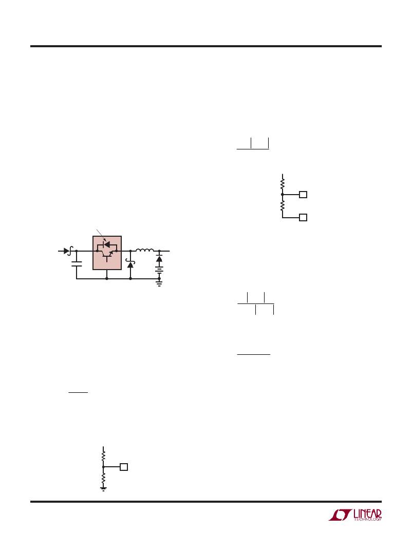
�shown� in� Figure� 4,� will� protect� the� LT1941� and� the� system�
�from� a� shorted� or� reversed� input.�
�R4�
�R3�
�NFB�
�FB3�
�1941� AI02�
�PARASITIC� DIODE�
�Use� 10k� or� larger,� up� to� 20k� for� R3.�
�V� IN�
�D4�
�V� IN�
�SW�
�V� OUT�
�Duty� Cycle� Range�
�LT1941�
�1941� F04�
�The� maximum� duty� cycle� (DC)� of� the� LT1941� inverter/boost�
�regulator� is� 77%.� The� duty� cycle� for� a� given� application�
�using� the� inverting� topology� is:�
�Figure� 4.� Diode� D4� Prevents� a� Shorted� Input� from�
�Discharging� a� Backup� Battery� Tied� to� the� Output�
�DC� =�
�V� OUT�
�V� IN� +� V� OUT�
�DC� =� OUT� IN�
�R� 3� =� R� 4� ?� OUT� –� 1� ?�
�INVERTER/BOOST CONSIDERATIONS�
�Regulating� Positive� Output� Voltages�
�The� output� voltage� is� programmed� with� a� resistor� divider�
�between� the� output� and� the� FB� pin.� Choose� the� resistors�
�according� to:�
�?� V� ?�
�?� 1� .� 25� V� ?�
�R4� should� be� 10k� or� less� to� avoid� bias� current� errors.�
�NFB� should� be� tied� to� FB3.�
�V� OUT�
�The� duty� cycle� for� a� given� application� using� the� boost�
�topology� is:�
�V� –� V�
�V� OUT�
�The� LT1941� can� still� be� used� in� applications� where� the�
�DC,� as� calculated� above,� is� above� 77%;� however,� the� part�
�must� be� operated� in� discontinuous� mode� so� that� the� actual�
�duty� cycle� is� reduced.�
�Inductor� Selection�
�Several� inductors� that� work� well� with� the� LT1941� inverter/�
�boost� regulator� are� listed� in� Table� 4.� Besides� these,� many�
�R3�
�R4�
�FB3�
�other� inductors� will� work.� Consult� each� manufacturer�
�for� detailed� information� and� for� their� entire� selection� of�
�related� parts.� Use� ferrite� core� inductors� to� obtain� the� best�
�ef?ciency.� When� using� coupled� inductors,� choose� one� that�
�1941� AI01�
�1941fb�
�14�
�相关PDF资料 |
PDF描述 |
|---|---|
| LT1942EUF#TRPBF | IC REG SW QUAD TFT LCD 24-QFN |
| LT1943EFE#TRPBF | IC REG SW QUAD TFT LCD 28-TSSOP |
| LT1944-1EMS#TR | IC REG BST ADJ 0.1A/175MA 10MSOP |
| LT1945IMS#TRPBF | IC REG MULTI CONFIG ADJ 10MSOP |
| LT1946EMS8E#TRPBF | IC REG BOOST 1.5A 8MSOP |
相关代理商/技术参数 |
参数描述 |
|---|---|
| LT1942 | 制造商:LINER 制造商全称:Linear Technology 功能描述:Quad DCDC Converter for Triple Outputs TFT Supply Plus LED Driver |
| LT1942EUF | 制造商:Linear Technology 功能描述:Conv DC-DC Quad Inv/Step Up 2.6V to 16V 24-Pin QFN EP |
| LT1942EUF#PBF | 功能描述:IC REG SW QUAD TFT LCD 24-QFN RoHS:是 类别:集成电路 (IC) >> PMIC - 稳压器 - 专用型 系列:- 标准包装:43 系列:- 应用:控制器,Intel VR11 输入电压:5 V ~ 12 V 输出数:1 输出电压:0.5 V ~ 1.6 V 工作温度:-40°C ~ 85°C 安装类型:表面贴装 封装/外壳:48-VFQFN 裸露焊盘 供应商设备封装:48-QFN(7x7) 包装:管件 |
| LT1942EUF#TRPBF | 功能描述:IC REG SW QUAD TFT LCD 24-QFN RoHS:是 类别:集成电路 (IC) >> PMIC - 稳压器 - 专用型 系列:- 标准包装:43 系列:- 应用:控制器,Intel VR11 输入电压:5 V ~ 12 V 输出数:1 输出电压:0.5 V ~ 1.6 V 工作温度:-40°C ~ 85°C 安装类型:表面贴装 封装/外壳:48-VFQFN 裸露焊盘 供应商设备封装:48-QFN(7x7) 包装:管件 |
| LT1942EUFPBF | 制造商:Linear Technology 功能描述:Conv DC-DC Quad Inv/Step-Up 16V QFN24EP |
发布紧急采购,3分钟左右您将得到回复。