- 您现在的位置:买卖IC网 > PDF目录44983 > LT1956-5EGN (LINEAR TECHNOLOGY CORP) 3 A SWITCHING REGULATOR, 570 kHz SWITCHING FREQ-MAX, PDSO16 PDF资料下载
参数资料
| 型号: | LT1956-5EGN |
| 厂商: | LINEAR TECHNOLOGY CORP |
| 元件分类: | 稳压器 |
| 英文描述: | 3 A SWITCHING REGULATOR, 570 kHz SWITCHING FREQ-MAX, PDSO16 |
| 封装: | 0.150 INCH, PLASTIC, SSOP-16 |
| 文件页数: | 9/24页 |
| 文件大小: | 437K |
| 代理商: | LT1956-5EGN |
17
LT1956/LT1956-5
APPLICATIO S I FOR ATIO
WU
UU
The VC and FB components should be kept as far away as
possible from the switch and boost nodes. The LT1956
pinout has been designed to aid in this. The ground for
these components should be separated from the switch
current path. Failure to do so will result in poor stability or
subharmonic like oscillation.
Board layout also has a significant effect on thermal
resistance. Pins 1, 8, 9 and 16, GND, are a continuous
copper plate that runs under the LT1956 die. This is the
best thermal path for heat out of the package. Reducing the
thermal resistance from Pins 1, 8, 9 and 16 onto the board
will reduce die temperature and increase the power capa-
bility of the LT1956. This is achieved by providing as much
copper area as possible around these pins. Adding mul-
tiple solder filled feedthroughs under and around these
four corner pins to the ground plane will also help. Similar
treatment to the catch diode and coil terminations will
reduce any additional heating effects.
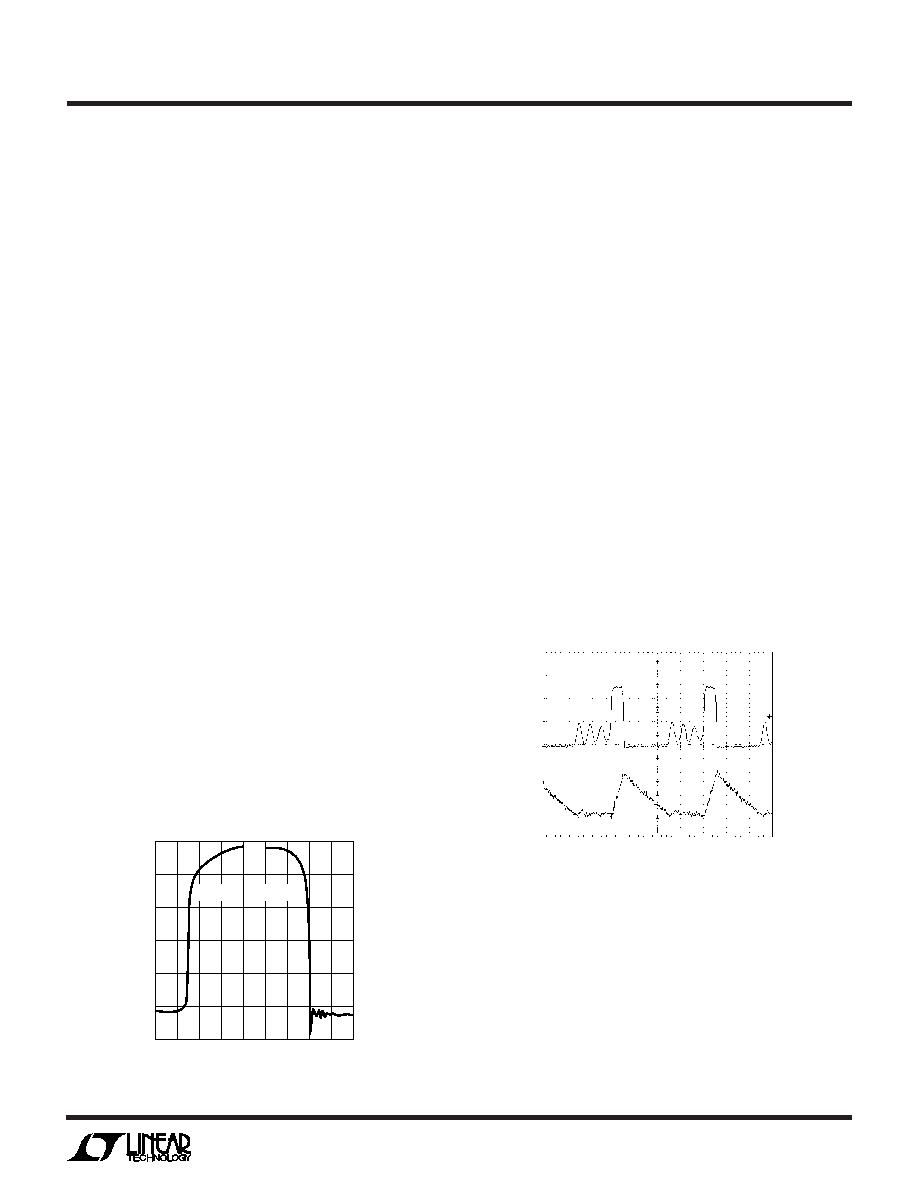
PARASITIC RESONANCE
Resonance or “ringing” may sometimes be seen on the
switch node (see Figure 7). Very high frequency ringing
following switch rise time is caused by switch/diode/input
capacitor lead inductance and diode capacitance. Schot-
tky diodes have very high “Q” junction capacitance that
can ring for many cycles when excited at high frequency.
If total lead length for the input capacitor, diode and switch
path is 1 inch, the inductance will be approximately 25nH.
At switch off, this will produce a spike across the NPN
output device in addition to the input voltage. At higher
Figure 7. Switch Node Resonance
currents this spike can be in the order of 10V to 20V or
higher with a poor layout, potentially exceeding the abso-
lute max switch voltage. The path around switch, catch
diode and input capacitor must be kept as short as
possible to ensure reliable operation. When looking at this,
a >100MHz oscilloscope must be used, and waveforms
should be observed on the leads of the package. This
switch off spike will also cause the SW node to go below
ground. The LT1956 has special circuitry inside which
mitigates this problem, but negative voltages over 0.8V
lasting longer than 10ns should be avoided. Note that
100MHz oscilloscopes are barely fast enough to see the
details of the falling edge overshoot in Figure 7.
A second, much lower frequency ringing is seen during
switch off time if load current is low enough to allow the
inductor current to fall to zero during part of the switch off
time (see Figure 8). Switch and diode capacitance reso-
nate with the inductor to form damped ringing at 1MHz to
10 MHz. This ringing is not harmful to the regulator and it
has not been shown to contribute significantly to EMI. Any
attempt to damp it with a resistive snubber will degrade
efficiency.
50ns/DIV
1956 F07
2V/DIV
SW RISE
SW FALL
SWITCH NODE
VOLTAGE
INDUCTOR
CURRENT AT
IOUT = 0.1A
VIN = 25V
500ns/DIV
1956 F08
VOUT = 5V
L = 15
H
Figure 8. Discontinuous Mode Ringing
THERMAL CALCULATIONS
Power dissipation in the LT1956 chip comes from four
sources: switch DC loss, switch AC loss, boost circuit
current, and input quiescent current. The following formu-
las show how to calculate each of these losses. These
formulas assume continuous mode operation, so they
should not be used for calculating efficiency at light load
currents.
10V/DIV
0.2A/DIV
相关PDF资料 |
PDF描述 |
|---|---|
| LT1956-5IGN | 3 A SWITCHING REGULATOR, 570 kHz SWITCHING FREQ-MAX, PDSO16 |
| LT1961IMS8E#TR | 3 A SWITCHING REGULATOR, 1500 kHz SWITCHING FREQ-MAX, PDSO8 |
| LT3092ITS8#PBF | SPECIALTY ANALOG CIRCUIT, PDSO8 |
| LT3092ETS8#TRPBF | SPECIALTY ANALOG CIRCUIT, PDSO8 |
| LT3092EST#PBF | SPECIALTY ANALOG CIRCUIT, PDSO3 |
相关代理商/技术参数 |
参数描述 |
|---|---|
| LT1956EFE | 功能描述:IC REG BUCK ADJ 1.5A 16TSSOP RoHS:否 类别:集成电路 (IC) >> PMIC - 稳压器 - DC DC 开关稳压器 系列:- 设计资源:Design Support Tool 标准包装:1 系列:- 类型:升压(升压) 输出类型:固定 输出数:1 输出电压:3V 输入电压:0.75 V ~ 2 V PWM 型:- 频率 - 开关:- 电流 - 输出:100mA 同步整流器:是 工作温度:-40°C ~ 85°C 安装类型:表面贴装 封装/外壳:SOT-23-5 细型,TSOT-23-5 包装:剪切带 (CT) 供应商设备封装:TSOT-23-5 其它名称:AS1323-BTTT-30CT |
| LT1956EFE#PBF | 功能描述:IC REG BUCK ADJ 1.5A 16TSSOP RoHS:是 类别:集成电路 (IC) >> PMIC - 稳压器 - DC DC 开关稳压器 系列:- 标准包装:250 系列:- 类型:降压(降压) 输出类型:固定 输出数:1 输出电压:1.2V 输入电压:2.05 V ~ 6 V PWM 型:电压模式 频率 - 开关:2MHz 电流 - 输出:500mA 同步整流器:是 工作温度:-40°C ~ 85°C 安装类型:表面贴装 封装/外壳:6-UFDFN 包装:带卷 (TR) 供应商设备封装:6-SON(1.45x1) 产品目录页面:1032 (CN2011-ZH PDF) 其它名称:296-25628-2 |
| LT1956EFE#TR | 功能描述:IC REG BUCK ADJ 1.5A 16TSSOP RoHS:否 类别:集成电路 (IC) >> PMIC - 稳压器 - DC DC 开关稳压器 系列:- 设计资源:Design Support Tool 标准包装:1 系列:- 类型:升压(升压) 输出类型:固定 输出数:1 输出电压:3V 输入电压:0.75 V ~ 2 V PWM 型:- 频率 - 开关:- 电流 - 输出:100mA 同步整流器:是 工作温度:-40°C ~ 85°C 安装类型:表面贴装 封装/外壳:SOT-23-5 细型,TSOT-23-5 包装:剪切带 (CT) 供应商设备封装:TSOT-23-5 其它名称:AS1323-BTTT-30CT |
| LT1956EFE#TRPBF | 功能描述:IC REG BUCK ADJ 1.5A 16TSSOP RoHS:是 类别:集成电路 (IC) >> PMIC - 稳压器 - DC DC 开关稳压器 系列:- 设计资源:Design Support Tool 标准包装:1 系列:- 类型:升压(升压) 输出类型:固定 输出数:1 输出电压:3V 输入电压:0.75 V ~ 2 V PWM 型:- 频率 - 开关:- 电流 - 输出:100mA 同步整流器:是 工作温度:-40°C ~ 85°C 安装类型:表面贴装 封装/外壳:SOT-23-5 细型,TSOT-23-5 包装:剪切带 (CT) 供应商设备封装:TSOT-23-5 其它名称:AS1323-BTTT-30CT |
| LT1956EFE-5 | 功能描述:IC REG BUCK 5V 1.5A 16TSSOP RoHS:否 类别:集成电路 (IC) >> PMIC - 稳压器 - DC DC 开关稳压器 系列:- 设计资源:Design Support Tool 标准包装:1 系列:- 类型:升压(升压) 输出类型:固定 输出数:1 输出电压:3V 输入电压:0.75 V ~ 2 V PWM 型:- 频率 - 开关:- 电流 - 输出:100mA 同步整流器:是 工作温度:-40°C ~ 85°C 安装类型:表面贴装 封装/外壳:SOT-23-5 细型,TSOT-23-5 包装:剪切带 (CT) 供应商设备封装:TSOT-23-5 其它名称:AS1323-BTTT-30CT |
发布紧急采购,3分钟左右您将得到回复。