- 您现在的位置:买卖IC网 > PDF目录13925 > LT1956IGN-5 (Linear Technology)IC REG BUCK 5V 1.5A 16SSOP PDF资料下载
参数资料
| 型号: | LT1956IGN-5 |
| 厂商: | Linear Technology |
| 文件页数: | 17/28页 |
| 文件大小: | 0K |
| 描述: | IC REG BUCK 5V 1.5A 16SSOP |
| 标准包装: | 100 |
| 类型: | 降压(降压) |
| 输出类型: | 固定 |
| 输出数: | 1 |
| 输出电压: | 5V |
| 输入电压: | 5.5 V ~ 60 V |
| PWM 型: | 电流模式 |
| 频率 - 开关: | 500kHz |
| 电流 - 输出: | 1.5A |
| 同步整流器: | 无 |
| 工作温度: | -40°C ~ 125°C |
| 安装类型: | 表面贴装 |
| 封装/外壳: | 16-SSOP(0.154",3.90mm 宽) |
| 包装: | 管件 |
| 供应商设备封装: | 16-SSOP |
| 其它名称: | LT1956IGN5 |
第1页第2页第3页第4页第5页第6页第7页第8页第9页第10页第11页第12页第13页第14页第15页第16页当前第17页第18页第19页第20页第21页第22页第23页第24页第25页第26页第27页第28页
�� �
�
�LT1956/LT1956-5�
�APPLICATIO� S� I� FOR� ATIO�
�LAYOUT� CONSIDERATIONS�
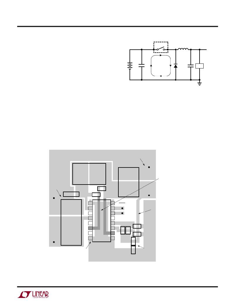
�As� with� all� high� frequency� switchers,� when� considering�
�layout,� care� must� be� taken� in� order� to� achieve� optimal�
�LT1956�
�L1�
�5V�
�electrical,� thermal� and� noise� performance.� For� maximum�
�efficiency,� switch� rise� and� fall� times� are� typically� in� the�
�nanosecond� range.� To� prevent� noise� both� radiated� and�
�V� IN�
�C3�
�HIGH�
�FREQUENCY�
�CIRCULATING�
�PATH�
�D1�
�C1�
�LOAD�
�conducted,� the� high� speed� switching� current� path,� shown�
�in� Figure� 5,� must� be� kept� as� short� as� possible.� This� is�
�implemented� in� the� suggested� layout� of� Figure� 6.� Shorten-�
�ing� this� path� will� also� reduce� the� parasitic� trace� inductance�
�of� approximately� 25nH/inch.� At� switch� off,� this� parasitic�
�inductance� produces� a� flyback� spike� across� the� LT1956�
�switch.� When� operating� at� higher� currents� and� input�
�voltages,� with� poor� layout,� this� spike� can� generate� volt-�
�ages� across� the� LT1956� that� may� exceed� its� absolute�
�maximum� rating.� A� ground� plane� should� always� be� used�
�under� the� switcher� circuitry� to� prevent� interplane� coupling�
�1956� F05�
�Figure� 5.� High� Speed� Switching� Path�
�The� V� C� and� FB� components� should� be� kept� as� far� away� as�
�possible� from� the� switch� and� boost� nodes.� The� LT1956�
�pinout� has� been� designed� to� aid� in� this.� The� ground� for�
�these� components� should� be� separated� from� the� switch�
�current� path.� Failure� to� do� so� will� result� in� poor� stability� or�
�subharmonic� like� oscillation.�
�and� overall� noise.�
�CONNECT� TO�
�GROUND� PLANE�
�GND�
�L1�
�FOR� THE� FE� PACKAGE,�
�MINIMIZE� LT1956�
�C1�
�SOLDER� THE� EXPOSED�
�PAD� TO� THE� COPPER�
�C3-D1� LOOP�
�GND�
�D1�
�C2�
�D2�
�V� OUT�
�GROUND� PLANE�
�UNDERNEATH� THE� DEVICE�
�GND�
�SW�
�GND�
�SHDN�
�KELVIN� SENSE�
�V� OUT�
�C3�
�V� IN�
�LT1956�
�FB�
�SYNC�
�BOOST�
�V� C�
�BIAS�
�R1� C� FB�
�R2�
�C� F�
�V� IN�
�GND�
�GND�
�R� C�
�KEEP� FB� AND� V� C� COMPONENTS�
�PLACE� FEEDTHROUGH� AROUND�
�C� C�
�AWAY� FROM� HIGH� FREQUENCY,�
�HIGH� CURRENT� COMPONENTS�
�GROUND� PINS� (4� CORNERS)� FOR�
�GOOD� THERMAL� CONDUCTIVITY�
�1956� F06�
�Figure� 6.� Suggested� Layout�
�1956f�
�17�
�相关PDF资料 |
PDF描述 |
|---|---|
| GEM40DCAH | CONN EDGECARD 80POS R/A .156 SLD |
| LT1766IGN-5 | IC REG BUCK 5V 1.5A 16SSOP |
| HM72A-12100LFTR13 | INDUCTOR 10UH HI PWR/PERF SMD |
| V150B28C150BF2 | CONVERTER MOD DC/DC 28V 150W |
| LT1766IGN | IC REG BUCK ADJ 1.5A 16SSOP |
相关代理商/技术参数 |
参数描述 |
|---|---|
| LT1956IGN-5#PBF | 功能描述:IC REG BUCK 5V 1.5A 16SSOP RoHS:是 类别:集成电路 (IC) >> PMIC - 稳压器 - DC DC 开关稳压器 系列:- 设计资源:Design Support Tool 标准包装:1 系列:- 类型:升压(升压) 输出类型:固定 输出数:1 输出电压:3V 输入电压:0.75 V ~ 2 V PWM 型:- 频率 - 开关:- 电流 - 输出:100mA 同步整流器:是 工作温度:-40°C ~ 85°C 安装类型:表面贴装 封装/外壳:SOT-23-5 细型,TSOT-23-5 包装:剪切带 (CT) 供应商设备封装:TSOT-23-5 其它名称:AS1323-BTTT-30CT |
| LT1956IGN-5#TR | 功能描述:IC REG BUCK 5V 1.5A 16SSOP RoHS:否 类别:集成电路 (IC) >> PMIC - 稳压器 - DC DC 开关稳压器 系列:- 设计资源:Design Support Tool 标准包装:1 系列:- 类型:升压(升压) 输出类型:固定 输出数:1 输出电压:3V 输入电压:0.75 V ~ 2 V PWM 型:- 频率 - 开关:- 电流 - 输出:100mA 同步整流器:是 工作温度:-40°C ~ 85°C 安装类型:表面贴装 封装/外壳:SOT-23-5 细型,TSOT-23-5 包装:剪切带 (CT) 供应商设备封装:TSOT-23-5 其它名称:AS1323-BTTT-30CT |
| LT1956IGN-5#TRPBF | 功能描述:IC REG BUCK 5V 1.5A 16SSOP RoHS:是 类别:集成电路 (IC) >> PMIC - 稳压器 - DC DC 开关稳压器 系列:- 设计资源:Design Support Tool 标准包装:1 系列:- 类型:升压(升压) 输出类型:固定 输出数:1 输出电压:3V 输入电压:0.75 V ~ 2 V PWM 型:- 频率 - 开关:- 电流 - 输出:100mA 同步整流器:是 工作温度:-40°C ~ 85°C 安装类型:表面贴装 封装/外壳:SOT-23-5 细型,TSOT-23-5 包装:剪切带 (CT) 供应商设备封装:TSOT-23-5 其它名称:AS1323-BTTT-30CT |
| LT1956IGNPBF | 制造商:Linear Technology 功能描述:DC-DC Converter Step-Down 5.5-60V SSOP16 |
| LT1959 | 制造商:LINER 制造商全称:Linear Technology 功能描述:4.5A, 500kHz Step-Down Switching Regulator |
发布紧急采购,3分钟左右您将得到回复。