- 您现在的位置:买卖IC网 > PDF目录14075 > LT1961IMS8E#PBF (Linear Technology)IC REG BOOST ADJ 1.5A 8MSOP PDF资料下载
参数资料
| 型号: | LT1961IMS8E#PBF |
| 厂商: | Linear Technology |
| 文件页数: | 10/16页 |
| 文件大小: | 0K |
| 描述: | IC REG BOOST ADJ 1.5A 8MSOP |
| 标准包装: | 50 |
| 类型: | 升压(升压) |
| 输出类型: | 可调式 |
| 输出数: | 1 |
| 输出电压: | 1.2 V ~ 35 V |
| 输入电压: | 3 V ~ 25 V |
| PWM 型: | 电流模式 |
| 频率 - 开关: | 1.25MHz |
| 电流 - 输出: | 1.5A |
| 同步整流器: | 无 |
| 工作温度: | -40°C ~ 125°C |
| 安装类型: | 表面贴装 |
| 封装/外壳: | 8-TSSOP,8-MSOP(0.118",3.00mm 宽)裸露焊盘 |
| 包装: | 管件 |
| 供应商设备封装: | 8-MSOP-EP |
�� �
�
�LT1961�
�APPLICATIO� N� S� I� N� FOR� M� ATIO� N�
�SYNCHRONIZATION�
�The� SYNC� pin,� is� used� to� synchronize� the� internal� oscilla-�
�tor� to� an� external� signal.� The� SYNC� input� must� pass� from�
�a� logic� level� low,� through� the� maximum� synchronization�
�threshold� with� a� duty� cycle� between� 20%� and� 80%.� The�
�input� can� be� driven� directly� from� a� logic� level� output.� The�
�synchronizing� range� is� equal� to� initial� operating� frequency�
�up� to� 2MHz.� This� means� that� minimum� practical� sync�
�frequency� is� equal� to� the� worst-case� high� self-oscillating�
�frequency� (1.5MHz),� not� the� typical� operating� frequency�
�of� 1.25MHz.� Caution� should� be� used� when� synchronizing�
�above� 1.7MHz� because� at� higher� sync� frequencies� the�
�amplitude� of� the� internal� slope� compensation� used� to�
�prevent� subharmonic� switching� is� reduced.� Higher� induc-�
�tor� values� will� tend� to� eliminate� this� problem.� See� Fre-�
�quency� Compensation� section� for� a� discussion� of� an�
�entirely� different� cause� of� subharmonic� switching� before�
�assuming� that� the� cause� is� insufficient� slope� compensa-�
�tion.� Application� Note� 19� has� more� details� on� the� theory�
�of� slope� compensation.�
�LAYOUT� CONSIDERATIONS�
�As� with� all� high� frequency� switchers,� when� considering�
�layout,� care� must� be� taken� to� achieve� optimal� electrical,�
�thermal� and� noise� performance.� For� maximum� efficiency,�
�switch� rise� and� fall� times� are� typically� in� the� nanosecond�
�range.� To� prevent� noise� both� radiated� and� conducted,� the�
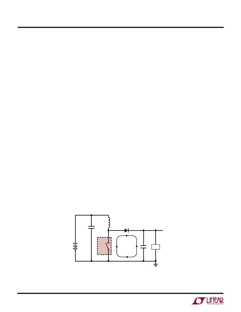
�L1�
�C3�
�high� speed� switching� current� path,� shown� in� Figure� 5,�
�must� be� kept� as� short� as� possible.� This� is� implemented� in�
�the� suggested� layout� of� Figure� 6.� Shortening� this� path� will�
�also� reduce� the� parasitic� trace� inductance� of� approxi-�
�mately� 25nH/inch.� At� switch� off,� this� parasitic� inductance�
�produces� a� flyback� spike� across� the� LT1961� switch.� When�
�operating� at� higher� currents� and� output� voltages,� with�
�poor� layout,� this� spike� can� generate� voltages� across� the�
�LT1961� that� may� exceed� its� absolute� maximum� rating.� A�
�ground� plane� should� always� be� used� under� the� switcher�
�circuitry� to� prevent� interplane� coupling� and� overall� noise.�
�The� V� C� and� FB� components� should� be� kept� as� far� away� as�
�possible� from� the� switch� node.� The� LT1961� pinout� has�
�been� designed� to� aid� in� this.� The� ground� for� these� compo-�
�nents� should� be� separated� from� the� switch� current� path.�
�Failure� to� do� so� will� result� in� poor� stability� or� subharmonic�
�like� oscillation.�
�Board� layout� also� has� a� significant� effect� on� thermal�
�resistance.� The� exposed� pad� is� the� copper� plate� that� runs�
�under� the� LT1961� die.� This� is� the� best� thermal� path� for� heat�
�out� of� the� package.� Soldering� the� pad� onto� the� board� will�
�reduce� die� temperature� and� increase� the� power� capability�
�of� the� LT1961.� Provide� as� much� copper� area� as� possible�
�around� this� pad.� Adding� multiple� solder� filled� feedthroughs�
�under� and� around� the� pad� to� the� ground� plane� will� also�
�help.� Similar� treatment� to� the� catch� diode� and� inductor�
�terminations� will� reduce� any� additional� heating� effects.�
�D1�
�V� OUT�
�SW�
�LT1961�
�HIGH�
�V� IN�
�FREQUENCY�
�SWITCHING�
�C1� LOAD�
�PATH�
�GND�
�1961� F05�
�Figure� 5.� High� Speed� Switching� Path�
�1961fa�
�10�
�相关PDF资料 |
PDF描述 |
|---|---|
| HM71-30331LFTR | HIGH PERF LOW COST INDUCTORS |
| MAX6869UK20D3S+T | IC MPU SUPERVISOR SOT23-5 |
| LTC3532EMS#TRPBF | IC REG BUCK BST SYNC 0.5A 10MSOP |
| HM71-30221LFTR | HIGH PERF LOW COST INDUCTORS |
| MAX6869UK20D4L+T | IC MPU SUPERVISOR SOT23-5 |
相关代理商/技术参数 |
参数描述 |
|---|---|
| LT1961IMS8ETR | 制造商:LINER 制造商全称:Linear Technology 功能描述:1.5A, 1.25MHz Step-Up Switching Regulator |
| LT1961IMS8ETRPBF | 制造商:LINER 制造商全称:Linear Technology 功能描述:1.5A, 1.25MHz Step-Up Switching Regulator |
| LT1962 | 制造商:LINER 制造商全称:Linear Technology 功能描述:Micropower Low Dropout Regulators with Shutdown |
| LT1962EMS8 | 功能描述:IC REG LDO ADJ .3A 8-MSOP RoHS:否 类别:集成电路 (IC) >> PMIC - 稳压器 - 线性 系列:- 产品培训模块:More Information on LDOs 标准包装:50 系列:- 稳压器拓扑结构:正,固定式 输出电压:3.3V 输入电压:最高 15V 电压 - 压降(标准):1.1V @ 800mA 稳压器数量:1 电流 - 输出:800mA 电流 - 限制(最小):800mA 工作温度:0°C ~ 125°C 安装类型:表面贴装 封装/外壳:TO-263-4,D²Pak(3 引线+接片),TO-263AA 供应商设备封装:D2PAK-3 包装:管件 |
| LT1962EMS8#PBF | 功能描述:IC REG LDO ADJ .3A 8-MSOP RoHS:是 类别:集成电路 (IC) >> PMIC - 稳压器 - 线性 系列:- 产品培训模块:MIC5365/66 Ultra-small LDO Regulators 标准包装:1 系列:- 稳压器拓扑结构:正,固定式 输出电压:3V 输入电压:最高 5.5V 电压 - 压降(标准):0.155V @ 150mA 稳压器数量:1 电流 - 输出:150mA 电流 - 限制(最小):200mA 工作温度:-40°C ~ 125°C 安装类型:表面贴装 封装/外壳:4-UDFN 裸露焊盘,4-TMLF? 供应商设备封装:4-TMLF?(1x1) 包装:Digi-Reel® 其它名称:576-3192-6 |
发布紧急采购,3分钟左右您将得到回复。