- 您现在的位置:买卖IC网 > PDF目录1823 > LT1962EMS8-1.8#TRPBF (Linear Technology)IC REG LDO 1.8V .3A 8MSOP PDF资料下载
参数资料
| 型号: | LT1962EMS8-1.8#TRPBF |
| 厂商: | Linear Technology |
| 文件页数: | 12/16页 |
| 文件大小: | 0K |
| 描述: | IC REG LDO 1.8V .3A 8MSOP |
| 产品培训模块: | More Information on LDOs |
| 标准包装: | 2,500 |
| 稳压器拓扑结构: | 正,固定式 |
| 输出电压: | 1.8V |
| 输入电压: | 最高 20V |
| 电压 - 压降(标准): | 0.27V @ 300mA |
| 稳压器数量: | 1 |
| 电流 - 输出: | 300mA |
| 电流 - 限制(最小): | 320mA |
| 工作温度: | -40°C ~ 125°C |
| 安装类型: | 表面贴装 |
| 封装/外壳: | 8-TSSOP,8-MSOP(0.118",3.00mm 宽) |
| 供应商设备封装: | 8-MSOP |
| 包装: | 带卷 (TR) |
| 配用: | DC1075A-ND - BOARD COMPANION |
�� �
�
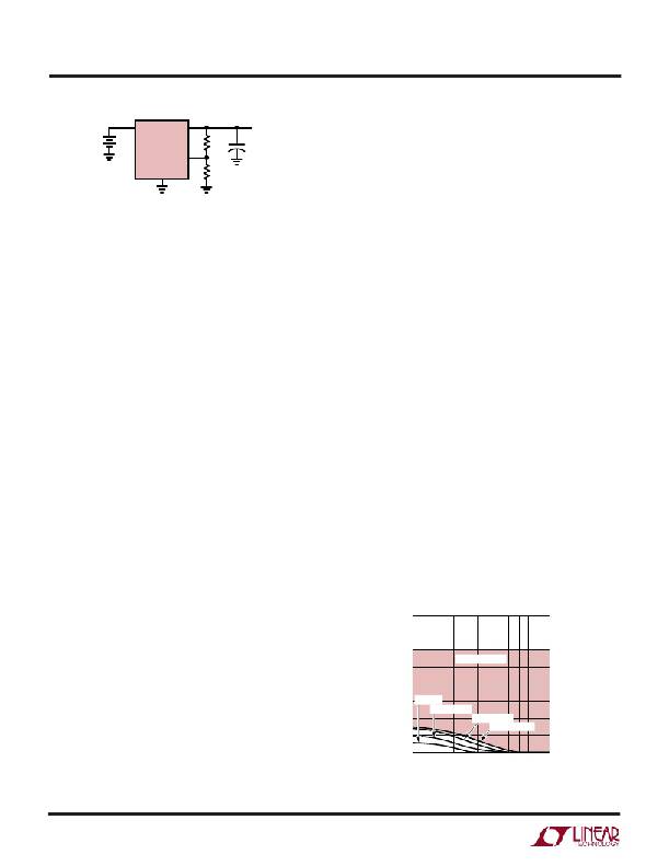
�LT1962� Series�
�APPLICATIO� S� I� FOR� ATIO�
�IN�
�OUT�
�V� OUT�
�(see� LT1962-5� Transient� Response� in� the� Typical� Perfor-�
�V� IN�
�LT1962�
�R2�
�+�
�mance� Characteristics).� However,� regulator� start-up� time�
�GND�
�ADJ�
�R1�
�1962� F02�
�is� inversely� proportional� to� the� size� of� the� bypass� capaci-�
�tor,� slowing� to� 15ms� with� a� 0.01� μ� F� bypass� capacitor� and�
�10� μ� F� output� capacitor.�
�V� OUT� =� 1� .� 22� V� ?� 1� +�
�?� +� (� I� ADJ� )(� R� 2� )�
�V� ADJ� =� 1� .� 22� V�
�?�
�?�
�R2� ?�
�R� 1� ?�
�Output� Capacitance� and� Transient� Response�
�The� LT1962� regulators� are� designed� to� be� stable� with� a�
�I� ADJ� =� 30� nA� AT� 25� °� C�
�OUTPUT� RANGE� =� 1.22V� TO� 20V�
�Figure� 2.� Adjustable� Operation�
�plus� the� ADJ� pin� bias� current.� The� ADJ� pin� bias� current,�
�30nA� at� 25� °� C,� flows� through� R2� into� the� ADJ� pin.� The�
�output� voltage� can� be� calculated� using� the� formula� in�
�Figure� 2.� The� value� of� R1� should� be� no� greater� than� 250k�
�to� minimize� errors� in� the� output� voltage� caused� by� the� ADJ�
�pin� bias� current.� Note� that� in� shutdown� the� output� is� turned�
�off� and� the� divider� current� will� be� zero.�
�The� adjustable� device� is� tested� and� specified� with� the� ADJ�
�pin� tied� to� the� OUT� pin� for� an� output� voltage� of� 1.22V.�
�Specifications� for� output� voltages� greater� than� 1.22V� will�
�be� proportional� to� the� ratio� of� the� desired� output� voltage� to�
�1.22V:� V� OUT� /1.22V.� For� example,� load� regulation� for� an�
�output� current� change� of� 1mA� to� 300mA� is� –� 2mV� typical�
�at� V� OUT� =� 1.22V.� At� V� OUT� =� 12V,� load� regulation� is:�
�(12V/1.22V)(–2mV)� =� –� 19.7mV�
�Bypass� Capacitance� and� Low� Noise� Performance�
�The� LT1962� regulators� may� be� used� with� the� addition� of� a�
�bypass� capacitor� from� V� OUT� to� the� BYP� pin� to� lower� output�
�voltage� noise.� A� good� quality� low� leakage� capacitor� is�
�recommended.� This� capacitor� will� bypass� the� reference� of�
�wide� range� of� output� capacitors.� The� ESR� of� the� output�
�capacitor� affects� stability,� most� notably� with� small� capaci-�
�tors.� A� minimum� output� capacitor� of� 3.3� μ� F� with� an� ESR� of�
�3� ?� or� less� is� recommended� to� prevent� oscillations.� The�
�LT1962-X� is� a� micropower� device� and� output� transient�
�response� will� be� a� function� of� output� capacitance.� Larger�
�values� of� output� capacitance� decrease� the� peak� deviations�
�and� provide� improved� transient� response� for� larger� load�
�current� changes.� Bypass� capacitors,� used� to� decouple�
�individual� components� powered� by� the� LT1962,� will� in-�
�crease� the� effective� output� capacitor� value.� With� larger�
�capacitors� used� to� bypass� the� reference� (for� low� noise�
�operation),� larger� values� of� output� capacitance� are� needed.�
�For� 100pF� of� bypass� capacitance,� 4.7� μ� F� of� output� capaci-�
�tor� is� recommended.� With� a� 1000pF� bypass� capacitor� or�
�larger,� a� 6.8� μ� F� output� capacitor� is� recommended.�
�The� shaded� region� of� Figure� 3� defines� the� range� over� which�
�the� LT1962� regulators� are� stable.� The� minimum� ESR�
�needed� is� defined� by� the� amount� of� bypass� capacitance�
�used,� while� the� maximum� ESR� is� 3� ?� .�
�Extra� consideration� must� be� given� to� the� use� of� ceramic�
�capacitors.� Ceramic� capacitors� are� manufactured� with� a�
�variety� of� dielectrics,� each� with� different� behavior� across�
�4.0�
�3.5�
�the� regulator,� providing� a� low� frequency� noise� pole.� The�
�noise� pole� provided� by� this� bypass� capacitor� will� lower� the�
�output� voltage� noise� to� as� low� as� 20� μ� V� RMS� with� the�
�addition� of� a� 0.01� μ� F� bypass� capacitor.� Using� a� bypass�
�capacitor� has� the� added� benefit� of� improving� transient�
�response.� With� no� bypass� capacitor� and� a� 10� μ� F� output�
�capacitor,� a� 10mA� to� 300mA� load� step� will� settle� to� within�
�1%� of� its� final� value� in� less� than� 100� μ� s.� With� the� addition�
�of� a� 0.01� μ� F� bypass� capacitor,� the� output� will� settle� to�
�within� 1%� for� a� 10mA� to� 300mA� load� step� in� less� than�
�10� μ� s,� with� total� output� voltage� deviation� of� less� than� 2%�
�3.0�
�2.5�
�2.0�
�1.5�
�1.0�
�0.5�
�0�
�1�
�STABLE REGION�
�C� BYP� =� 0�
�C� BYP� = 100pF�
�C� BYP� = 330pF�
�C� BYP� ≥� 1000pF�
�2� 3� 4� 5� 6� 7� 8� 9� 10�
�OUTPUT� CAPACITANCE� (� μ� F)�
�1962� F03�
�Figure� 3.� Stability�
�12�
�相关PDF资料 |
PDF描述 |
|---|---|
| LT1963AMPQ#TRPBF | IC REG LDO ADJ 1.5A 5-DD |
| LT1964IDD#TRPBF | IC REG LDO NEG ADJ .2A 8DFN |
| LT1965EQ-1.8#PBF | IC REG LDO 1.8V 1.1A 5-DDPAK |
| LT1976HFE#TRPBF | IC REG BUCK ADJ 1.5A 16TSSOP |
| LT1977IFE#TRPBF | IC REG BUCK ADJ 1.5A 16TSSOP |
相关代理商/技术参数 |
参数描述 |
|---|---|
| LT1962EMS8-2.5 | 功能描述:IC REG LDO 2.5V .3A 8-MSOP RoHS:否 类别:集成电路 (IC) >> PMIC - 稳压器 - 线性 系列:- 产品培训模块:More Information on LDOs 标准包装:50 系列:- 稳压器拓扑结构:正,固定式 输出电压:3.3V 输入电压:最高 15V 电压 - 压降(标准):1.1V @ 800mA 稳压器数量:1 电流 - 输出:800mA 电流 - 限制(最小):800mA 工作温度:0°C ~ 125°C 安装类型:表面贴装 封装/外壳:TO-263-4,D²Pak(3 引线+接片),TO-263AA 供应商设备封装:D2PAK-3 包装:管件 |
| LT1962EMS8-2.5#PBF | 功能描述:IC REG LDO 2.5V .3A 8-MSOP RoHS:是 类别:集成电路 (IC) >> PMIC - 稳压器 - 线性 系列:- 产品培训模块:MIC5365/66 Ultra-small LDO Regulators 标准包装:1 系列:- 稳压器拓扑结构:正,固定式 输出电压:3V 输入电压:最高 5.5V 电压 - 压降(标准):0.155V @ 150mA 稳压器数量:1 电流 - 输出:150mA 电流 - 限制(最小):200mA 工作温度:-40°C ~ 125°C 安装类型:表面贴装 封装/外壳:4-UDFN 裸露焊盘,4-TMLF? 供应商设备封装:4-TMLF?(1x1) 包装:Digi-Reel® 其它名称:576-3192-6 |
| LT1962EMS8-2.5#PBF | 制造商:Linear Technology 功能描述:IC VOLT REG FIXED +2.5V BIPOLAR TS |
| LT1962EMS8-2.5#TR | 功能描述:IC REG LDO 2.5V .3A 8-MSOP RoHS:否 类别:集成电路 (IC) >> PMIC - 稳压器 - 线性 系列:- 产品培训模块:More Information on LDOs 标准包装:50 系列:- 稳压器拓扑结构:正,固定式 输出电压:3.3V 输入电压:最高 15V 电压 - 压降(标准):1.1V @ 800mA 稳压器数量:1 电流 - 输出:800mA 电流 - 限制(最小):800mA 工作温度:0°C ~ 125°C 安装类型:表面贴装 封装/外壳:TO-263-4,D²Pak(3 引线+接片),TO-263AA 供应商设备封装:D2PAK-3 包装:管件 |
| LT1962EMS8-2.5#TRPBF | 功能描述:IC REG LDO 2.5V .3A 8-MSOP RoHS:是 类别:集成电路 (IC) >> PMIC - 稳压器 - 线性 系列:- 产品培训模块:More Information on LDOs 标准包装:50 系列:- 稳压器拓扑结构:正,固定式 输出电压:3.3V 输入电压:最高 15V 电压 - 压降(标准):1.1V @ 800mA 稳压器数量:1 电流 - 输出:800mA 电流 - 限制(最小):800mA 工作温度:0°C ~ 125°C 安装类型:表面贴装 封装/外壳:TO-263-4,D²Pak(3 引线+接片),TO-263AA 供应商设备封装:D2PAK-3 包装:管件 |
发布紧急采购,3分钟左右您将得到回复。