参数资料
| 型号: | LT1962EMS8-5#PBF |
| 厂商: | Linear Technology |
| 文件页数: | 11/16页 |
| 文件大小: | 0K |
| 描述: | IC REG LDO 5V .3A 8-MSOP |
| 产品培训模块: | More Information on LDOs |
| 标准包装: | 50 |
| 稳压器拓扑结构: | 正,固定式 |
| 输出电压: | 5V |
| 输入电压: | 最高 20V |
| 电压 - 压降(标准): | 0.27V @ 300mA |
| 稳压器数量: | 1 |
| 电流 - 输出: | 300mA |
| 电流 - 限制(最小): | 320mA |
| 工作温度: | -40°C ~ 125°C |
| 安装类型: | 表面贴装 |
| 封装/外壳: | 8-TSSOP,8-MSOP(0.118",3.00mm 宽) |
| 供应商设备封装: | 8-MSOP |
| 包装: | 管件 |
| 产品目录页面: | 1329 (CN2011-ZH PDF) |
| 配用: | DC1075A-ND - BOARD COMPANION |
�� �
�
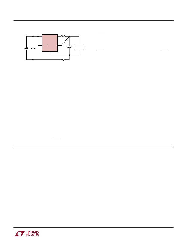
�LT1962� Series�
�PI� FU� CTIO� S�
�V� IN�
�+�
�8�
�5�
�IN� OUT�
�LT1962�
�SHDN� SENSE�
�GND�
�4�
�1�
�2�
�R� P�
�R� P�
�+�
�LOAD�
�1962� F01�
�SHDN� pin� can� be� driven� either� by� 5V� logic� or� open-�
�collector� logic� with� a� pull-up� resistor.� The� pull-up� resistor�
�is� required� to� supply� the� pull-up� current� of� the� open-�
�collector� gate,� normally� several� microamperes,� and� the�
�SHDN� pin� current,� typically� 1� μ� A.� If� unused,� the� SHDN� pin�
�must� be� connected� to� V� IN� .� The� device� will� not� function� if�
�the� SHDN� pin� is� not� connected.�
�Figure� 1.� Kelvin� Sense� Connection�
�pin.� The� ADJ� pin� voltage� is� 1.22V� referenced� to� ground� and�
�the� output� voltage� range� is� 1.22V� to� 20V.�
�BYP� (Pin� 3):� Bypass.� The� BYP� pin� is� used� to� bypass� the�
�reference� of� the� LT1962� to� achieve� low� noise� performance�
�from� the� regulator.� The� BYP� pin� is� clamped� internally� to�
�±� 0.6V� (one� V� BE� ).� A� small� capacitor� from� the� output� to� this�
�pin� will� bypass� the� reference� to� lower� the� output� voltage�
�noise.� A� maximum� value� of� 0.01� μ� F� can� be� used� for�
�reducing� output� voltage� noise� to� a� typical� 20� μ� V� RMS� over� a�
�10Hz� to� 100kHz� bandwidth.� If� not� used,� this� pin� must� be�
�left� unconnected.�
�GND� (Pin� 4):� Ground.�
�SHDN� (Pin� 5):� Shutdown.� The� SHDN� pin� is� used� to� put� the�
�LT1962� regulators� into� a� low� power� shutdown� state.� The�
�output� will� be� off� when� the� SHDN� pin� is� pulled� low.� The�
�APPLICATIO� S� I� FOR� ATIO�
�The� LT1962� series� are� 300mA� low� dropout� regulators� with�
�micropower� quiescent� current� and� shutdown.� The� devices�
�are� capable� of� supplying� 300mA� at� a� dropout� voltage� of�
�300mV.� Output� voltage� noise� can� be� lowered� to� 20� μ� V� RMS�
�over� a� 10Hz� to� 100kHz� bandwidth� with� the� addition� of� a�
�0.01� μ� F� reference� bypass� capacitor.� Additionally,� the� refer-�
�ence� bypass� capacitor� will� improve� transient� response� of�
�the� regulator,� lowering� the� settling� time� for� transient� load�
�conditions.� The� low� operating� quiescent� current� (30� μ� A)�
�drops� to� less� than� 1� μ� A� in� shutdown.� In� addition� to� the� low�
�quiescent� current,� the� LT1962� regulators� incorporate� sev-�
�eral� protection� features� which� make� them� ideal� for� use� in�
�battery-powered� systems.� The� devices� are� protected�
�against� both� reverse� input� and� reverse� output� voltages.� In�
�battery� backup� applications� where� the� output� can� be� held�
�NC� (Pins� 6,� 7):� No� Connect.� These� pins� are� not� internally�
�connected.� For� improved� power� handling� capabilities,�
�these� pins� can� be� connected� to� the� PC� board.�
�IN� (Pin� 8):� Input.� Power� is� supplied� to� the� device� through�
�the� IN� pin.� A� bypass� capacitor� is� required� on� this� pin� if� the�
�device� is� more� than� six� inches� away� from� the� main� input�
�filter� capacitor.� In� general,� the� output� impedance� of� a�
�battery� rises� with� frequency,� so� it� is� advisable� to� include� a�
�bypass� capacitor� in� battery-powered� circuits.� A� bypass�
�capacitor� in� the� range� of� 1� μ� F� to� 10� μ� F� is� sufficient.� The�
�LT1962� regulators� are� designed� to� withstand� reverse�
�voltages� on� the� IN� pin� with� respect� to� ground� and� the� OUT�
�pin.� In� the� case� of� a� reverse� input,� which� can� happen� if� a�
�battery� is� plugged� in� backwards,� the� device� will� act� as� if�
�there� is� a� diode� in� series� with� its� input.� There� will� be� no�
�reverse� current� flow� into� the� regulator� and� no� reverse�
�voltage� will� appear� at� the� load.� The� device� will� protect� both�
�itself� and� the� load.�
�up� by� a� backup� battery� when� the� input� is� pulled� to� ground,�
�the� LT1962-X� acts� like� it� has� a� diode� in� series� with� its�
�output� and� prevents� reverse� current� flow.� Additionally,� in�
�dual� supply� applications� where� the� regulator� load� is� re-�
�turned� to� a� negative� supply,� the� output� can� be� pulled� below�
�ground� by� as� much� as� 20V� and� still� allow� the� device� to� start�
�and� operate.�
�Adjustable� Operation�
�The� adjustable� version� of� the� LT1962� has� an� output�
�voltage� range� of� 1.22V� to� 20V.� The� output� voltage� is� set� by�
�the� ratio� of� two� external� resistors� as� shown� in� Figure� 2.� The�
�device� servos� the� output� to� maintain� the� ADJ� pin� voltage�
�at� 1.22V� referenced� to� ground.� The� current� in� R1� is� then�
�equal� to� 1.22V/R1� and� the� current� in� R2� is� the� current� in� R1�
�11�
�相关PDF资料 |
PDF描述 |
|---|---|
| ABM24DTMD | CONN EDGECARD 48POS R/A .156 SLD |
| 450VXR150MEFCSN25X50 | CAP ALUM 150UF 450V 20% SNAP-IN |
| GCM30DCBI-S189 | CONN EDGECARD 60POS R/A .156 SLD |
| ACM15DRST-S664 | CONN EDGECARD 30POS DIP .156 SLD |
| GCM30DCCI-S189 | CONN EDGECARD 60POS R/A .156 SLD |
相关代理商/技术参数 |
参数描述 |
|---|---|
| LT1962EMS8PBF | 制造商:Linear Technology 功能描述: 制造商:Linear Technology 功能描述:LDO Regulator Adj. 300mA Low Noise MSOP8 |
| LT1963 | 制造商:LINER 制造商全称:Linear Technology 功能描述:1.5A, Low Noise, Fast Transient Response LDO Regulators |
| LT1963/ | 制造商:LINER 制造商全称:Linear Technology 功能描述:45V VIN, Micropower, Low Noise, 100mA Low Dropout, Linear Regulator |
| LT1963A | 制造商:LINER 制造商全称:Linear Technology 功能描述:1.1A, Low Noise, Low Dropout Linear Regulator |
| LT1963A_1208 | 制造商:LINER 制造商全称:Linear Technology 功能描述:1.5A Low Noise Fast Transient Response LDO Regulators |
发布紧急采购,3分钟左右您将得到回复。