- 您现在的位置:买卖IC网 > PDF目录2155 > LT1969CMS#TRPBF (Linear Technology)IC OP-AMP ADJ CURRNT DUAL 10MSOP PDF资料下载
参数资料
| 型号: | LT1969CMS#TRPBF |
| 厂商: | Linear Technology |
| 文件页数: | 4/20页 |
| 文件大小: | 0K |
| 描述: | IC OP-AMP ADJ CURRNT DUAL 10MSOP |
| 标准包装: | 2,500 |
| 放大器类型: | 通用 |
| 电路数: | 2 |
| 转换速率: | 200 V/µs |
| 增益带宽积: | 700MHz |
| 电流 - 输入偏压: | 1.5µA |
| 电压 - 输入偏移: | 1000µV |
| 电流 - 电源: | 7mA |
| 电流 - 输出 / 通道: | 700mA |
| 电压 - 电源,单路/双路(±): | 4 V ~ 13 V,±2 V ~ 6.5 V |
| 工作温度: | 0°C ~ 70°C |
| 安装类型: | 表面贴装 |
| 封装/外壳: | 10-TFSOP,10-MSOP(0.118",3.00mm 宽) |
| 供应商设备封装: | 10-MSOP |
| 包装: | 带卷 (TR) |
12
LT1969
Capacitive Loading
The LT1969 is stable with a 1000pF capacitive load. The
photo of the small-signal response with 1000pF load in a
gain of 10 shows 50% overshoot. The photo of the large-
signal response with a 1000pF load shows that the output
slew rate is not limited by the short-circuit current. The
Typical Performance Curve of Frequency Response vs
Capacitive Load shows the peaking for various capacitive
loads.
This stability is useful in the case of directly driving a
coaxial cable or twisted pair that is inadvertently
unterminated. For best pulse fidelity, however, a termina-
tion resistor of value equal to the characteristic impedance
of the cable or twisted pair (i.e., 50
/75/100/135)
should be placed in series with the output. The other end
of the cable or twisted pair should be terminated with the
same value resistor to ground.
APPLICATIO S I FOR ATIO
WU
UU
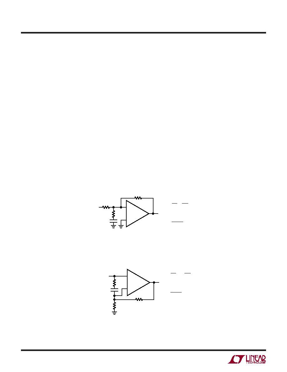
Figure 2. Compensation for Inverting Gains
RG
RC
Vo
Vi
CC
(OPTIONAL)
–
+
1969 F02
RF
=
–RF
RG
Vo
Vi
< 15MHz
1
2
πRCCC
(RC || RG) ≤ RF/9
Figure 3. Compensation for Noninverting Gains
RC
Vo
Vi
CC
(OPTIONAL)
+
–
1969 F03
RF
RG
= 1 +
RF
RG
Vo
Vi
< 15MHz
1
2
πRCCC
(RC || RG) ≤ RF/9
Compensation
The LT1969 is stable in a gain 10 or higher for any supply
and resistive load. It is easily compensated for lower gains
with a single resistor or a resistor plus a capacitor.
Figure 2 shows that for inverting gains, a resistor from the
inverting node to AC ground guarantees stability if the
parallel combination of RC and RG is less than or equal to
RF/9. For lowest distortion and DC output offset, a series
capacitor, CC, can be used to reduce the noise gain at lower
frequencies. The break frequency produced by RC and CC
should be less than 15MHz to minimize peaking. The
Typical Curve of Frequency Response vs Supply Voltage,
AV = –1 shows less than 1dB of peaking for a break
frequency of 12.8MHz.
Figure 3 shows compensation in the noninverting configu-
ration. The RC, CC network acts similarly to the inverting
case. The input impedance is not reduced because the
相关PDF资料 |
PDF描述 |
|---|---|
| LT1970IFE#TRPBF | IC OP AMP 500MA ADJ 20-TSSOP |
| LT1990AHS8#TRPBF | IC AMP DIFF +/-250V MCRPWR 8SOIC |
| LT1993CUD-10#TRPBF | IC DIFF AMP/ADC DRVR 16-QFN |
| LT1993CUD-2#PBF | IC DIFF AMP/ADC DRVR 16-QFN |
| LT1993CUD-4#TRPBF | IC DIFF AMP/ADC DRVR 16-QFN |
相关代理商/技术参数 |
参数描述 |
|---|---|
| LT1970 | 制造商:LINER 制造商全称:Linear Technology 功能描述:500mA Power Op Amp with Adjustable Precision Current Limit |
| LT1970_1 | 制造商:LINER 制造商全称:Linear Technology 功能描述:500mA Power Op Amp with Adjustable Precision Current Limit |
| LT1970A | 制造商:LINER 制造商全称:Linear Technology 功能描述:500mA Power Op Amp with Adjustable Precision Current Limit |
| LT1970ACFE#PBF | 功能描述:IC OP AMP 500MA ADJ CURR 20TSSOP RoHS:是 类别:集成电路 (IC) >> Linear - Amplifiers - Instrumentation 系列:- 标准包装:50 系列:- 放大器类型:J-FET 电路数:2 输出类型:- 转换速率:3.5 V/µs 增益带宽积:1MHz -3db带宽:- 电流 - 输入偏压:30pA 电压 - 输入偏移:2000µV 电流 - 电源:200µA 电流 - 输出 / 通道:- 电压 - 电源,单路/双路(±):7 V ~ 36 V,±3.5 V ~ 18 V 工作温度:0°C ~ 70°C 安装类型:通孔 封装/外壳:8-DIP(0.300",7.62mm) 供应商设备封装:8-PDIP 包装:管件 |
| LT1970ACFE#TRPBF | 功能描述:IC OP AMP 500MA ADJ CURR 20TSSOP RoHS:是 类别:集成电路 (IC) >> Linear - Amplifiers - Instrumentation 系列:- 标准包装:50 系列:- 放大器类型:J-FET 电路数:2 输出类型:- 转换速率:3.5 V/µs 增益带宽积:1MHz -3db带宽:- 电流 - 输入偏压:30pA 电压 - 输入偏移:2000µV 电流 - 电源:200µA 电流 - 输出 / 通道:- 电压 - 电源,单路/双路(±):7 V ~ 36 V,±3.5 V ~ 18 V 工作温度:0°C ~ 70°C 安装类型:通孔 封装/外壳:8-DIP(0.300",7.62mm) 供应商设备封装:8-PDIP 包装:管件 |
发布紧急采购,3分钟左右您将得到回复。