- 您现在的位置:买卖IC网 > PDF目录2155 > LT1969CMS#TRPBF (Linear Technology)IC OP-AMP ADJ CURRNT DUAL 10MSOP PDF资料下载
参数资料
| 型号: | LT1969CMS#TRPBF |
| 厂商: | Linear Technology |
| 文件页数: | 5/20页 |
| 文件大小: | 0K |
| 描述: | IC OP-AMP ADJ CURRNT DUAL 10MSOP |
| 标准包装: | 2,500 |
| 放大器类型: | 通用 |
| 电路数: | 2 |
| 转换速率: | 200 V/µs |
| 增益带宽积: | 700MHz |
| 电流 - 输入偏压: | 1.5µA |
| 电压 - 输入偏移: | 1000µV |
| 电流 - 电源: | 7mA |
| 电流 - 输出 / 通道: | 700mA |
| 电压 - 电源,单路/双路(±): | 4 V ~ 13 V,±2 V ~ 6.5 V |
| 工作温度: | 0°C ~ 70°C |
| 安装类型: | 表面贴装 |
| 封装/外壳: | 10-TFSOP,10-MSOP(0.118",3.00mm 宽) |
| 供应商设备封装: | 10-MSOP |
| 包装: | 带卷 (TR) |
13
LT1969
network is bootstrapped. This network can also be placed
between the inverting input and an AC ground.
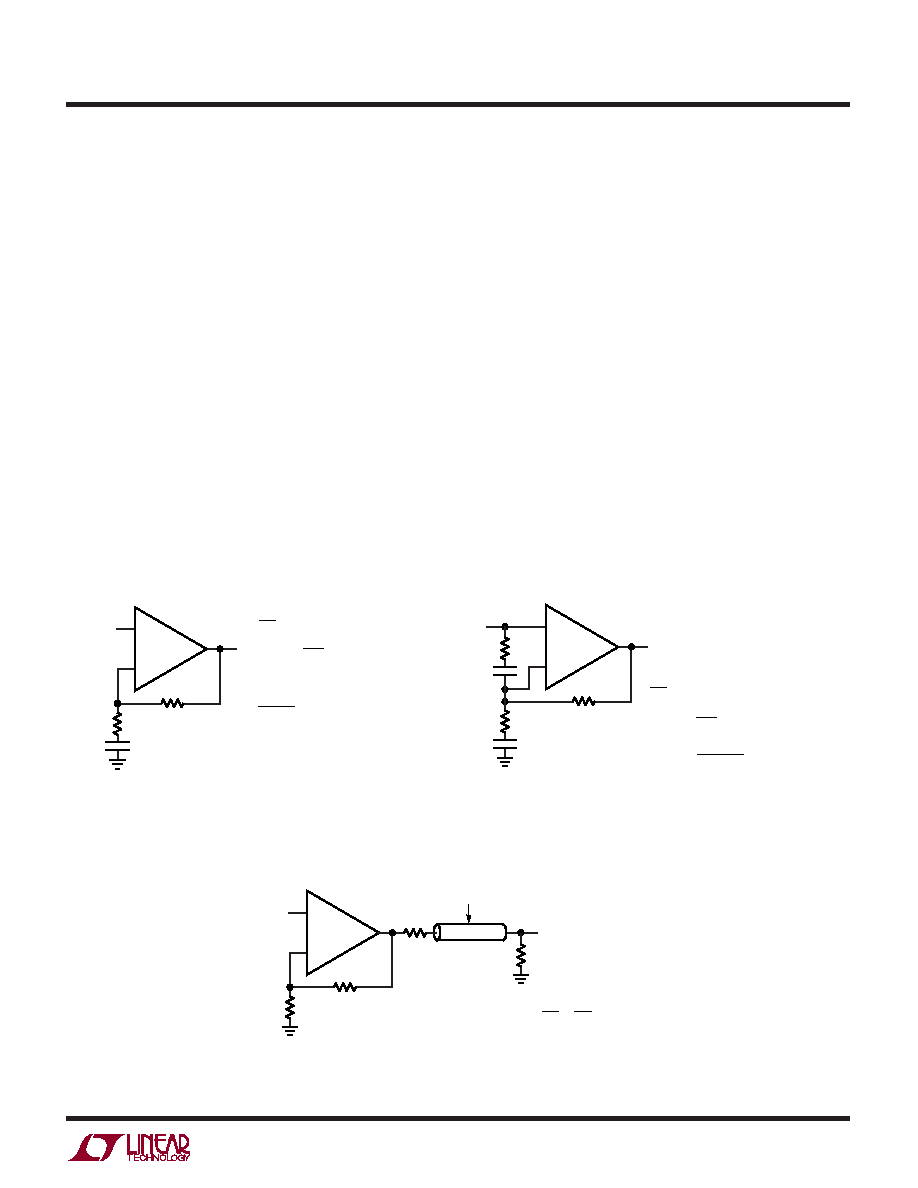
Another compensation scheme for noninverting circuits is
shown in Figure 4. The circuit is unity gain at low frequency
and a gain of 1 + RF/RG at high frequency. The DC output
offset is reduced by a factor of ten. The techniques of
Figures 3 and 4 can be combined as shown in Figure 5. The
gain is unity at low frequencies, 1 + RF/RG at mid-band and
for stability, a gain of 10 or greater at high frequencies.
Output Loading
The LT1969 output stage is very wide bandwidth and able
to source and sink large currents. Reactive loading, even
isolated with a back-termination resistor, can cause ring-
ing at frequencies of hundreds of MHz. For this reason, any
design should be evaluated over a wide range of output
conditions. To reduce the effects of reactive loading, an
optional snubber network consisting of a series RC across
the load can provide a resistive load at high frequency.
Another option is to filter the drive to the load. If a back-
termination resistor is used, a capacitor to ground at the
load can eliminate ringing.
Line Driving Back-Termination
The standard method of cable or line back-termination is
shown in Figure 6. The cable/line is terminated in its
characteristic impedance (50
, 75, 100, 135, etc.).
A back-termination resistor also equal to to the
chararacteristic impedance should be used for maximum
pulse fidelity of outgoing signals, and to terminate the line
for incoming signals in a full-duplex application. There are
three main drawbacks to this approach. First, the power
dissipated in the load and back-termination resistors is
equal so half of the power delivered by the amplifier is
Figure 5. Combination Compensation
RC
Vo
Vi
CC
+
–
1969 F05
RF
RG
CBIG
RF
RG
= 1 AT LOW FREQUENCIES
= 1 +
AT MEDIUM FREQUENCIES
RF
(RC || RG)
= 1 +
AT HIGH FREQUENCIES
Vo
Vi
Figure 4. Alternate Noninverting Compensation
+
–
1969 F04
RF
RG
Vi
VO
CC
< 15MHz
1
2
πRGCC
RG ≤ RF/9
= 1 (LOW FREQUENCIES)
(HIGH FREQUENCIES)
Vo
Vi
= 1 +
RF
RG
Figure 6. Standard Cable/Line Back-Termination
+
–
1969 F06
RF
RBT
CABLE OR LINE WITH
CHARACTERISTIC IMPEDANCE RL
RG
VO
Vi
RL
(1 + RF/RG)
=
Vo
Vi
1
2
RBT = RL
APPLICATIO S I FOR ATIO
WU
UU
相关PDF资料 |
PDF描述 |
|---|---|
| LT1970IFE#TRPBF | IC OP AMP 500MA ADJ 20-TSSOP |
| LT1990AHS8#TRPBF | IC AMP DIFF +/-250V MCRPWR 8SOIC |
| LT1993CUD-10#TRPBF | IC DIFF AMP/ADC DRVR 16-QFN |
| LT1993CUD-2#PBF | IC DIFF AMP/ADC DRVR 16-QFN |
| LT1993CUD-4#TRPBF | IC DIFF AMP/ADC DRVR 16-QFN |
相关代理商/技术参数 |
参数描述 |
|---|---|
| LT1970 | 制造商:LINER 制造商全称:Linear Technology 功能描述:500mA Power Op Amp with Adjustable Precision Current Limit |
| LT1970_1 | 制造商:LINER 制造商全称:Linear Technology 功能描述:500mA Power Op Amp with Adjustable Precision Current Limit |
| LT1970A | 制造商:LINER 制造商全称:Linear Technology 功能描述:500mA Power Op Amp with Adjustable Precision Current Limit |
| LT1970ACFE#PBF | 功能描述:IC OP AMP 500MA ADJ CURR 20TSSOP RoHS:是 类别:集成电路 (IC) >> Linear - Amplifiers - Instrumentation 系列:- 标准包装:50 系列:- 放大器类型:J-FET 电路数:2 输出类型:- 转换速率:3.5 V/µs 增益带宽积:1MHz -3db带宽:- 电流 - 输入偏压:30pA 电压 - 输入偏移:2000µV 电流 - 电源:200µA 电流 - 输出 / 通道:- 电压 - 电源,单路/双路(±):7 V ~ 36 V,±3.5 V ~ 18 V 工作温度:0°C ~ 70°C 安装类型:通孔 封装/外壳:8-DIP(0.300",7.62mm) 供应商设备封装:8-PDIP 包装:管件 |
| LT1970ACFE#TRPBF | 功能描述:IC OP AMP 500MA ADJ CURR 20TSSOP RoHS:是 类别:集成电路 (IC) >> Linear - Amplifiers - Instrumentation 系列:- 标准包装:50 系列:- 放大器类型:J-FET 电路数:2 输出类型:- 转换速率:3.5 V/µs 增益带宽积:1MHz -3db带宽:- 电流 - 输入偏压:30pA 电压 - 输入偏移:2000µV 电流 - 电源:200µA 电流 - 输出 / 通道:- 电压 - 电源,单路/双路(±):7 V ~ 36 V,±3.5 V ~ 18 V 工作温度:0°C ~ 70°C 安装类型:通孔 封装/外壳:8-DIP(0.300",7.62mm) 供应商设备封装:8-PDIP 包装:管件 |
发布紧急采购,3分钟左右您将得到回复。