参数资料
| 型号: | LT3027IDD#TRPBF |
| 厂商: | Linear Technology |
| 文件页数: | 9/16页 |
| 文件大小: | 0K |
| 描述: | IC REG LDO ADJ .1A 10-DFN |
| 产品培训模块: | More Information on LDOs |
| 标准包装: | 2,500 |
| 稳压器拓扑结构: | 正,可调式 |
| 输出电压: | 1.22 V ~ 20 V |
| 输入电压: | 1.8 V ~ 20 V |
| 电压 - 压降(标准): | 0.3V @ 100mA |
| 稳压器数量: | 2 |
| 电流 - 输出: | 100mA |
| 电流 - 限制(最小): | 110mA |
| 工作温度: | -40°C ~ 125°C |
| 安装类型: | 表面贴装 |
| 封装/外壳: | 10-WFDFN 裸露焊盘 |
| 供应商设备封装: | 10-DFN(3x3) |
| 包装: | 带卷 (TR) |
�� �
�
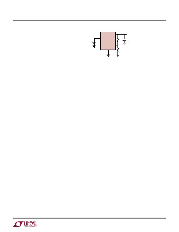
�LT3027�
�APPLICATIO� S� I� FOR� ATIO�
�?� +� (� I� ADJ� )(� R� 2� )�
�V� OUT� =� 1� .� 22� V� ?� 1� +�
�The LT3027 is a dual 100mA low dropout regulator with�
�independent� inputs,� micropower� quiescent� current� and�
�shutdown.� The� device� is� capable� of� supplying� 100mA� per�
�channel� at� a� dropout� voltage� of� 300mV.� Output� voltage�
�noise� can� be� lowered� to� 20� μ� V� RMS� over� a� 10Hz� to� 100kHz�
�bandwidth� with� the� addition� of� a� 0.01� μ� F� reference� bypass�
�capacitor.� Additionally,� the� reference� bypass� capacitor� will�
�V� IN�
�IN�
�OUT�
�LT3027�
�ADJ�
�GND�
�+�
�R2�
�R1�
�3027� F01�
�V� OUT�
�?� R2� ?�
�?� R� 1� ?�
�V� ADJ� =� 1� .� 22� V�
�I� ADJ� =� 30� nA� AT� 25� °� C�
�OUTPUT� RANGE� =� 1� .� 22� V� TO� 20� V�
�improve� transient� response� of� the� regulator,� lowering� the�
�settling� time� for� transient� load� conditions.� The� low� oper-�
�ating� quiescent� current� (25� μ� A� per� channel)� drops� to� less�
�than� 1� μ� A� in� shutdown.� In� addition� to� the� low� quiescent�
�current,� the� LT3027� regulator� incorporates� several� pro-�
�tection� features� which� make� it� ideal� for� use� in� battery-�
�powered� systems.� The� device� is� protected� against� reverse�
�input� voltages.� Additionally,� in� dual� supply� applications�
�where� the� regulator� load� is� returned� to� a� negative� supply,�
�the� output� can� be� pulled� below� ground� by� as� much� as� 20V�
�and� still� allow� the� device� to� start� and� operate.�
�Adjustable� Operation�
�The� LT3027� has� an� output� voltage� range� of� 1.22V� to� 20V.�
�The� output� voltage� is� set� by� the� ratio� of� two� external� resis-�
�tors� as� shown� in� Figure� 1.� The� device� servos� the� output� to�
�maintain� the� corresponding� ADJ� pin� voltage� at� 1.22V� ref-�
�erenced� to� ground.� The� current� in� R1� is� then� equal� to� 1.22V/�
�R1� and� the� current� in� R2� is� the� current� in� R1� plus� the� ADJ�
�pin� bias� current.� The� ADJ� pin� bias� current,� 30nA� at� 25� °� C,�
�flows� through� R2� into� the� ADJ� pin.� The� output� voltage� can�
�be� calculated� using� the� formula� in� Figure� 1.� The� value� of� R1�
�should� be� no� greater� than� 250k� to� minimize� errors� in� the�
�output� voltage� caused� by� the� ADJ� pin� bias� current.� Note� that�
�in� shutdown� the� output� is� turned� off� and� the� divider� current�
�will� be� zero.� Curves� of� ADJ� Pin� Voltage� vs� Temperature� and�
�ADJ� Pin� Bias� Current� vs� Temperature� appear� in� the� Typical�
�Performance� Characteristics.�
�Figure� 1.� Adjustable� Operation�
�The� device� is� tested� and� specified� with� the� ADJ� pin� tied� to�
�the� corresponding� OUT� pin� for� an� output� voltage� of� 1.22V.�
�Specifications� for� output� voltages� greater� than� 1.22V� will�
�be� proportional� to� the� ratio� of� the� desired� output� voltage� to�
�1.22V:� V� OUT� /1.22V.� For� example,� load� regulation� for� an�
�output� current� change� of� 1mA� to� 100mA� is� –1mV� typical�
�at� V� OUT� =� 1.22V.� At� V� OUT� =� 12V,� load� regulation� is:�
�(12V/1.22V)(–1mV)� =� –� 9.8mV�
�Bypass� Capacitance� and� Low� Noise� Performance�
�The� LT3027� regulator� may� be� used� with� the� addition� of� a�
�bypass� capacitor� from� V� OUT� to� the� corresponding� BYP� pin�
�to� lower� output� voltage� noise.� A� good� quality� low� leakage�
�capacitor� is� recommended.� This� capacitor� will� bypass� the�
�reference� of� the� regulator,� providing� a� low� frequency� noise�
�pole.� The� noise� pole� provided� by� this� bypass� capacitor� will�
�lower� the� output� voltage� noise� to� as� low� as� 20� μ� V� RMS� with�
�the� addition� of� a� 0.01� μ� F� bypass� capacitor.� Using� a� bypass�
�capacitor� has� the� added� benefit� of� improving� transient�
�response.� With� no� bypass� capacitor� and� a� 10� μ� F� output�
�capacitor,� a� 10mA� to� 100mA� load� step� will� settle� to� within�
�1%� of� its� final� value� in� less� than� 100� μ� s.� With� the� addition�
�of� a� 0.01� μ� F� bypass� capacitor,� the� output� will� stay� within�
�1%� for� a� 10mA� to� 100mA� load� step� (see� Transient� Reponse�
�in� Typical� Performance� Characteristics� section).� However,�
�regulator� start-up� time� is� inversely� proportional� to� the� size�
�of� the� bypass� capacitor,� slowing� to� 15ms� with� a� 0.01� μ� F�
�bypass� capacitor� and� 10� μ� F� output� capacitor.�
�3027fa�
�9�
�相关PDF资料 |
PDF描述 |
|---|---|
| LT3028IDHC#TRPBF | IC REG LDO ADJ .5A/.1A 16-DFN |
| LT3029MPMSE#TRPBF | IC REG LDO ADJ .5A 16MSOP |
| LT3032MPDE-5#TRPBF | IC REG LDO +-5V .15A 14-DFN |
| LT3050MPMSE-5#TRPBF | IC REG LDO 5V .1A 12-MSOP |
| LT3060MPTS8-5#TRPBF | IC REG LDO 5V .1A TSOT23-8 |
相关代理商/技术参数 |
参数描述 |
|---|---|
| LT3027IMSE | 制造商:Linear Technology 功能描述:LDO Regulator Pos 1.22V to 20V1.22V to 20V 0.1A/0.1A 10-Pin MSOP EP |
| LT3027IMSE#PBF | 功能描述:IC REG LDO ADJ .1A 10-MSOP RoHS:是 类别:集成电路 (IC) >> PMIC - 稳压器 - 线性 系列:- 产品培训模块:More Information on LDOs 标准包装:50 系列:- 稳压器拓扑结构:正,固定式 输出电压:3.3V 输入电压:最高 15V 电压 - 压降(标准):1.1V @ 800mA 稳压器数量:1 电流 - 输出:800mA 电流 - 限制(最小):800mA 工作温度:0°C ~ 125°C 安装类型:表面贴装 封装/外壳:TO-263-4,D²Pak(3 引线+接片),TO-263AA 供应商设备封装:D2PAK-3 包装:管件 |
| LT3027IMSE#TRPBF | 功能描述:IC REG LDO ADJ .1A 10-MSOP RoHS:是 类别:集成电路 (IC) >> PMIC - 稳压器 - 线性 系列:- 产品培训模块:More Information on LDOs 标准包装:50 系列:- 稳压器拓扑结构:正,固定式 输出电压:3.3V 输入电压:最高 15V 电压 - 压降(标准):1.1V @ 800mA 稳压器数量:1 电流 - 输出:800mA 电流 - 限制(最小):800mA 工作温度:0°C ~ 125°C 安装类型:表面贴装 封装/外壳:TO-263-4,D²Pak(3 引线+接片),TO-263AA 供应商设备封装:D2PAK-3 包装:管件 |
| LT3028 | 制造商:LINER 制造商全称:Linear Technology 功能描述:1.1A, Low Noise, Low Dropout Linear Regulator |
| LT3028EDHC | 制造商:LINER 制造商全称:Linear Technology 功能描述:Dual 100mA/500mA Low Dropout, Low Noise,Micropower Regulators with Independent Inputs |
发布紧急采购,3分钟左右您将得到回复。