- 您现在的位置:买卖IC网 > PDF目录13837 > LT3431IFE (Linear Technology)IC REG BUCK ADJ 3A 16TSSOP PDF资料下载
参数资料
| 型号: | LT3431IFE |
| 厂商: | Linear Technology |
| 文件页数: | 21/28页 |
| 文件大小: | 0K |
| 描述: | IC REG BUCK ADJ 3A 16TSSOP |
| 标准包装: | 95 |
| 类型: | 降压(降压) |
| 输出类型: | 可调式 |
| 输出数: | 1 |
| 输出电压: | 1.2 V ~ 48 V |
| 输入电压: | 5.5 V ~ 60 V |
| PWM 型: | 电流模式 |
| 频率 - 开关: | 500kHz |
| 电流 - 输出: | 3A |
| 同步整流器: | 无 |
| 工作温度: | -40°C ~ 125°C |
| 安装类型: | 表面贴装 |
| 封装/外壳: | 16-TSSOP(0.173",4.40mm)裸露焊盘 |
| 包装: | 管件 |
| 供应商设备封装: | 16-TSSOP-EP |
第1页第2页第3页第4页第5页第6页第7页第8页第9页第10页第11页第12页第13页第14页第15页第16页第17页第18页第19页第20页当前第21页第22页第23页第24页第25页第26页第27页第28页
�� �
�
�LT3431�
�APPLICATIO� S� I� FOR� ATIO�
�A� detailed� theoretical� basis� for� estimating� internal� power�
�dissipation� is� given� in� the� Thermal� Calculations� section.�
�This� will� allow� a� first� pass� check� of� whether� an� application’s�
�maximum� input� voltage� requirement� is� suitable� for� the�
�LT3431.� Be� aware� that� these� calculations� are� for� DC� input�
�voltages� and� that� input� voltage� transients� as� high� as� 60V�
�are� possible� if� the� resulting� increase� in� internal� power�
�dissipation� is� of� insufficient� time� duration� to� raise� die�
�temperature� significantly.� For� the� FE� package,� this� means�
�high� voltage� transients� on� the� order� of� hundreds� of� milli-�
�seconds� are� possible.� If� LT3431� thermal� calculations�
�show� power� dissipation� is� not� suitable� for� the� given�
�tion,� the� theoretical� analysis� considers� only� first� order�
�non-ideal� component� behavior.� For� these� reasons,� it� is�
�important� that� a� final� stability� check� is� made� with� produc-�
�tion� layout� and� components.�
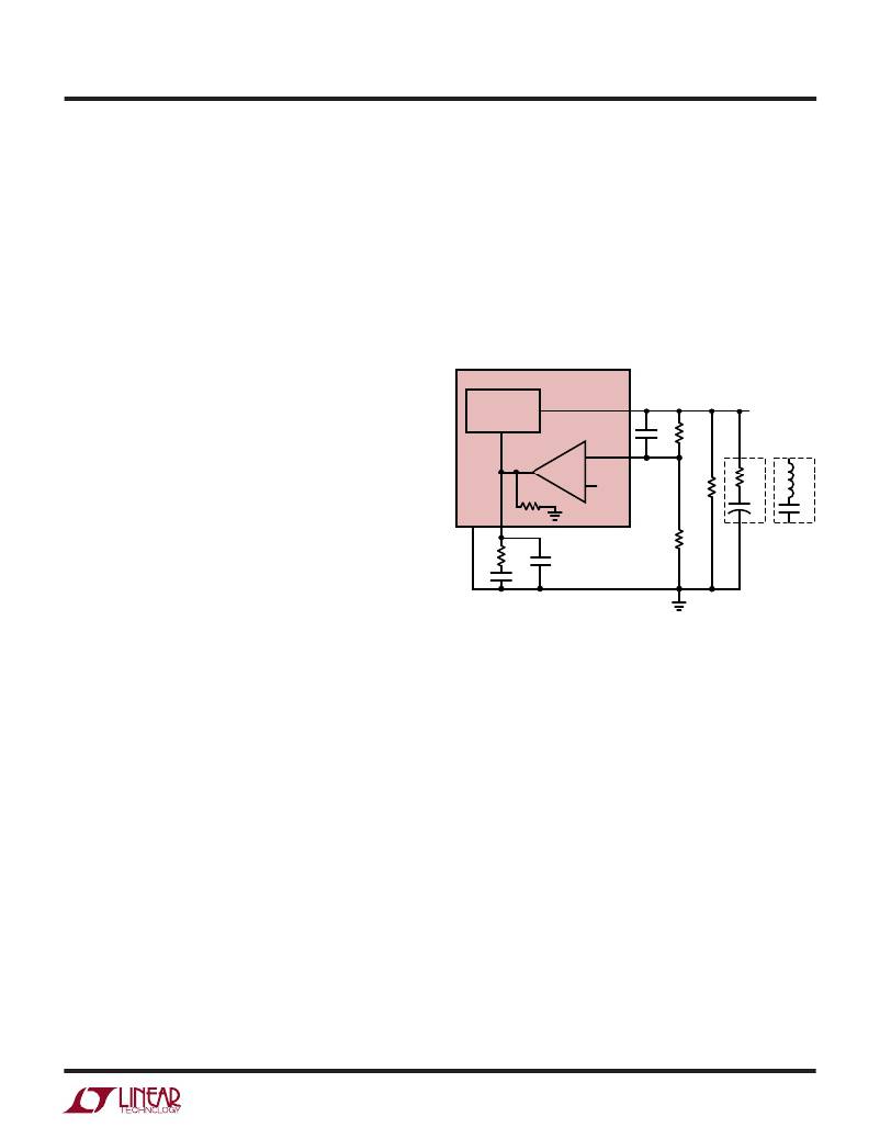
�The� LT3431� uses� current� mode� control.� This� alleviates�
�many� of� the� phase� shift� problems� associated� with� the�
�inductor.� The� basic� regulator� loop� is� shown� in� Figure� 10.�
�The� LT3431� can� be� considered� as� two� g� m� blocks,� the� error�
�amplifier� and� the� power� stage.�
�LT3431�
�application,� the� LT3430� is� a� recommended� alternative�
�CURRENT� MODE�
�POWER� STAGE�
�SW�
�OUTPUT�
�since� it� is� identical� to� the� LT3431� but� runs� cooler� at�
�200kHz.�
�g� m� =� 2mho�
�ERROR�
�AMPLIFIER�
�FB�
�C� FB�
�R1�
�CERAMIC�
�Switch� minimum� on� time� is� the� other� factor� that� may� limit�
�the� maximum� operational� input� voltage� for� the� LT3431� if�
�R� O�
�200k�
�g� m� =�
�2000� μ� mho�
�1.22V�
�R� LOAD�
�+�
�ESR�
�ESL�
�pulse-skipping� behavior� is� not� allowed.� For� the� LT3431,�
�pulse-skipping� may� occur� for� V� IN� /(V� OUT� +� V� F� )� ratios� >� 4.�
�(V� F� =� Schottky� diode� D1� forward� voltage� drop,� Figure� 5.)�
�If� the� LT3430� is� used,� the� ratio� increases� to� 10.� Pulse-�
�GND�
�V� C�
�R� C�
�C� C�
�C� F�
�R2�
�C1�
�TANTALUM�
�C1�
�skipping� is� the� regulator’s� way� of� missing� switch� pulses� to�
�maintain� output� voltage� regulation.� Although� an� increase�
�in� output� ripple� voltage� can� occur� during� pulse-skipping,�
�a� ceramic� output� capacitor� can� be� used� to� keep� ripple�
�voltage� to� a� minimum� (see� output� ripple� voltage� compari-�
�son� for� tantalum� vs� ceramic� output� capacitors,� Figure� 3).�
�FREQUENCY� COMPENSATION�
�Before� starting� on� the� theoretical� analysis� of� frequency�
�response,� the� following� should� be� remembered—the� worse�
�the� board� layout,� the� more� difficult� the� circuit� will� be� to�
�stabilize.� This� is� true� of� almost� all� high� frequency� analog�
�circuits,� read� the� Layout� Considerations� section� first.�
�Common� layout� errors� that� appear� as� stability� problems�
�are� distant� placement� of� input� decoupling� capacitor� and/�
�or� catch� diode,� and� connecting� the� V� C� compensation� to� a�
�ground� track� carrying� significant� switch� current.� In� addi-�
�3431� F10�
�Figure� 10.� Model� for� Loop� Response�
�Figure� 11� shows� the� overall� loop� response.� At� the� V� C� pin,�
�the� frequency� compensation� components� used� are:�
�R� C� =� 3.3k,� C� C� =� 0.022� μ� F� and� C� F� =� 220pF.� The� output�
�capacitor� used� is� a� 100� μ� F,� 10V� tantalum� capacitor� with�
�typical� ESR� of� 100m� ?� .�
�The� ESR� of� the� tantalum� output� capacitor� provides� a�
�useful� zero� in� the� loop� frequency� response� for� maintain-�
�ing� stability.�
�This� ESR,� however,� contributes� significantly� to� the� ripple�
�voltage� at� the� output� (see� Output� Ripple� Voltage� in� the�
�Applications� Information� section).� It� is� possible� to� reduce�
�capacitor� size� and� output� ripple� voltage� by� replacing� the�
�sn3431� 3431fs�
�21�
�相关PDF资料 |
PDF描述 |
|---|---|
| L06038R2DGWTR | INDUCTOR THIN FILM 8.2NH 0603 |
| LT3690IUFE#TRPBF | IC REG BUCK SYNC ADJ 4A 26QFN |
| L06038R2DFWTR | INDUCTOR THIN FILM 8.2NH 0603 |
| LT1171HVCT#30PBF | IC REG MULTI CONFIG ADJ TO220-5 |
| L06036R8DGWTR | INDUCTOR THIN FILM 6.8NH 0603 |
相关代理商/技术参数 |
参数描述 |
|---|---|
| LT3431IFE#PBF | 功能描述:IC REG BUCK ADJ 3A 16TSSOP RoHS:是 类别:集成电路 (IC) >> PMIC - 稳压器 - DC DC 开关稳压器 系列:- 产品培训模块:MIC23xxx HyperLight Load™ Regulators 标准包装:5,000 系列:HyperLight Load® 类型:降压(降压) 输出类型:固定 输出数:1 输出电压:1.8V 输入电压:2.7 V ~ 5.5 V PWM 型:混合物 频率 - 开关:4MHz 电流 - 输出:2A 同步整流器:是 工作温度:-40°C ~ 125°C 安装类型:表面贴装 封装/外壳:8-VFDFN 裸露焊盘,8-MLF? 包装:带卷 (TR) 供应商设备封装:8-MLF?(2x2) 产品目录页面:1094 (CN2011-ZH PDF) 其它名称:576-3303-2 |
| LT3431IFE#PBF | 制造商:Linear Technology 功能描述:IC STEP-DOWN REGULATOR 16-TSSOP 制造商:Linear Technology 功能描述:IC, STEP-DOWN REGULATOR, 16-TSSOP |
| LT3431IFE#TR | 功能描述:IC REG BUCK ADJ 3A 16TSSOP RoHS:否 类别:集成电路 (IC) >> PMIC - 稳压器 - DC DC 开关稳压器 系列:- 设计资源:Design Support Tool 标准包装:1 系列:- 类型:升压(升压) 输出类型:固定 输出数:1 输出电压:3V 输入电压:0.75 V ~ 2 V PWM 型:- 频率 - 开关:- 电流 - 输出:100mA 同步整流器:是 工作温度:-40°C ~ 85°C 安装类型:表面贴装 封装/外壳:SOT-23-5 细型,TSOT-23-5 包装:剪切带 (CT) 供应商设备封装:TSOT-23-5 其它名称:AS1323-BTTT-30CT |
| LT3431IFE#TRPBF | 功能描述:IC REG BUCK ADJ 3A 16TSSOP RoHS:是 类别:集成电路 (IC) >> PMIC - 稳压器 - DC DC 开关稳压器 系列:- 设计资源:Design Support Tool 标准包装:1 系列:- 类型:升压(升压) 输出类型:固定 输出数:1 输出电压:3V 输入电压:0.75 V ~ 2 V PWM 型:- 频率 - 开关:- 电流 - 输出:100mA 同步整流器:是 工作温度:-40°C ~ 85°C 安装类型:表面贴装 封装/外壳:SOT-23-5 细型,TSOT-23-5 包装:剪切带 (CT) 供应商设备封装:TSOT-23-5 其它名称:AS1323-BTTT-30CT |
| LT3433 | 制造商:LINER 制造商全称:Linear Technology 功能描述:High Voltage Step-Up/Step-Down DC/DC Converter |
发布紧急采购,3分钟左右您将得到回复。