- 您现在的位置:买卖IC网 > PDF目录13971 > LT3433EFE#TRPBF (Linear Technology)IC REG BUCK BST ADJ 0.5A 16TSSOP PDF资料下载
参数资料
| 型号: | LT3433EFE#TRPBF |
| 厂商: | Linear Technology |
| 文件页数: | 5/16页 |
| 文件大小: | 0K |
| 描述: | IC REG BUCK BST ADJ 0.5A 16TSSOP |
| 标准包装: | 2,500 |
| 类型: | 降压(降压),升压(升压) |
| 输出类型: | 可调式 |
| 输出数: | 1 |
| 输出电压: | 3.3 V ~ 20 V |
| 输入电压: | 4 V ~ 60 V |
| PWM 型: | 电流模式,混合 |
| 频率 - 开关: | 200kHz |
| 电流 - 输出: | 500mA |
| 同步整流器: | 无 |
| 工作温度: | -40°C ~ 125°C |
| 安装类型: | 表面贴装 |
| 封装/外壳: | 16-TSSOP(0.173",4.40mm)裸露焊盘 |
| 包装: | 带卷 (TR) |
| 供应商设备封装: | 16-TSSOP-EP |
�� �
�
�LT3433�
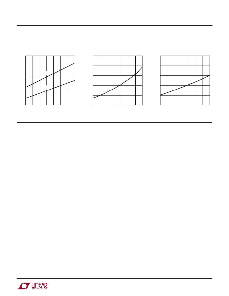
�TYPICAL� PERFOR� A� CE� CHARACTERISTICS�
�1.1�
�1.0�
�0.9�
�Switch� Resistance�
�vs� Temperature� (I� SW� =� 500mA)�
�40�
�37�
�V� BST� Supply� Switch� Drive� Current�
�vs� Temperature� (I� SW� =� 500mA)�
�40�
�37�
�V� OUT� Supply� Switch� Drive� Current�
�vs� Temperature� (I� SW� =� 500mA)�
�0.8�
�0.7�
�R� SWH�
�R� SWL�
�34�
�31�
�34�
�31�
�0.6�
�0.5�
�28�
�28�
�0.4�
�–50� –25�
�0�
�25�
�50�
�75�
�100�
�125�
�25�
�–50�
�–25�
�0�
�25�
�50�
�75�
�100�
�125�
�25�
�–50�
�–25�
�0�
�25�
�50�
�75�
�100�
�125�
�TEMPERATURE� (� °� C)�
�PI� FU� CTIO� S�
�3433� G12�
�TEMPERATURE� (� °� C)�
�3433� G13�
�TEMPERATURE� (� °� C)�
�3433� G14�
�SGND� (Pins� 1,� 8,� 9,� 16):� Low� Noise� Ground� Reference.�
�V� BST� (Pin� 2):� Boosted� Switch� Supply.� This� “boosted”� sup-�
�ply� rail� is� referenced� to� the� SW_H� pin.� Supply� voltage� is�
�maintained� by� a� bootstrap� capacitor� tied� from� the� V� BST� pin�
�to� the� SW_H� pin.� A� 1� μ� F� capacitor� is� generally� adequate� for�
�most� applications.�
�The� charge� on� the� bootstrap� capacitor� is� refreshed� through�
�a� diode,� typically� connected� from� the� converter� output�
�(V� OUT� ),� during� the� switch-off� period.� Minimum� off-time�
�operation� assures� that� the� boost� capacitor� is� refreshed� each�
�switch� cycle.� The� LT3433� supports� operational� V� BST� sup-�
�ply� voltages� up� to� 75V� (absolute� maximum)� as� referenced�
�to� ground.�
�SW_H� (Pin� 3):� Boosted� Switch� Output.� This� is� the� current�
�return� for� the� boosted� switch� and� corresponds� to� the� emitter�
�of� the� switch� transistor.� The� boosted� switch� shorts� the�
�SW_H� pin� to� the� V� IN� supply� when� enabled.� The� drive� cir-�
�cuitry� for� this� switch� is� boosted� above� the� V� IN� supply�
�through� the� V� BST� pin,� allowing� saturation� of� the� switch� for�
�maximum� efficiency.� The� “ON”� resistance� of� the� boosted�
�switch� is� 0.8� ?� .�
�V� IN� (Pin� 4):� Input� Power� Supply.� This� pin� supplies� power�
�to� the� boosted� switch� and� corresponds� to� the� collector� of�
�the� switch� transistor.This� pin� also� supplies� power� to� most�
�of� the� IC’s� internal� circuitry� if� the� V� BIAS� pin� is� not� driven�
�externally.� This� supply� will� be� subject� to� high� switching�
�transient� currents� so� this� pin� requires� a� high� quality� bypass�
�capacitor� that� meets� whatever� application-specific� input�
�ripple� current� requirements� exist.�
�BURST_EN� (Pin� 5):� Burst� Mode� Enable/Disable.� When�
�this� pin� is� below� 0.3V,� Burst� Mode� operation� is� enabled.�
�Pin� input� bias� current� <� 1� μ� A� when� Burst� Mode� operation�
�is� enabled.� If� Burst� Mode� operation� is� not� desired,� pulling�
�this� pin� above� 2V� will� disable� the� burst� function.� When�
�Burst� Mode� operation� is� disabled,� typical� pin� input� current�
�=� 35� μ� A.� BURST_EN� should� not� be� pulled� above� 20V.� This�
�pin� is� typically� shorted� to� SGND� for� Burst� Mode� function,�
�or� connected� to� either� V� BIAS� or� V� OUT� to� disable� Burst� Mode�
�operation.�
�V� C� (Pin� 6):� Error� Amplifier� Output.� The� voltage� on� the� V� C�
�pin� corresponds� to� the� maximum� switch� current� per� oscil-�
�lator� cycle.� The� error� amplifier� is� typically� configured� as� an�
�integrator� circuit� by� connecting� an� RC� network� from� this�
�pin� to� ground.� This� circuit� typically� creates� the� dominant�
�pole� for� the� converter� regulation� feedback� loop.� Specific� in-�
�tegrator� characteristics� can� be� configured� to� optimize� tran-�
�sient� response.� See� Applications� Information.�
�3433f�
�5�
�相关PDF资料 |
PDF描述 |
|---|---|
| HM61-20270LFTR13 | INJECTION MOULDED INDUCTORS |
| ESM31DTKS | CONN EDGECARD 62POS DIP .156 SLD |
| AIAP-03-561-K | INDUCTOR 560UH 10% 1.17A |
| EMM28DTKN | CONN EDGECARD 56POS DIP .156 SLD |
| AIAP-03-471-K | INDUCTOR 470UH 10% 1.24A |
相关代理商/技术参数 |
参数描述 |
|---|---|
| LT3433IFE | 功能描述:IC REG BUCK BST ADJ 0.5A 16TSSOP RoHS:否 类别:集成电路 (IC) >> PMIC - 稳压器 - DC DC 开关稳压器 系列:- 设计资源:Design Support Tool 标准包装:1 系列:- 类型:升压(升压) 输出类型:固定 输出数:1 输出电压:3V 输入电压:0.75 V ~ 2 V PWM 型:- 频率 - 开关:- 电流 - 输出:100mA 同步整流器:是 工作温度:-40°C ~ 85°C 安装类型:表面贴装 封装/外壳:SOT-23-5 细型,TSOT-23-5 包装:剪切带 (CT) 供应商设备封装:TSOT-23-5 其它名称:AS1323-BTTT-30CT |
| LT3433IFE#PBF | 功能描述:IC REG BUCK BST ADJ 0.5A 16TSSOP RoHS:是 类别:集成电路 (IC) >> PMIC - 稳压器 - DC DC 开关稳压器 系列:- 设计资源:Design Support Tool 标准包装:1 系列:- 类型:升压(升压) 输出类型:固定 输出数:1 输出电压:3V 输入电压:0.75 V ~ 2 V PWM 型:- 频率 - 开关:- 电流 - 输出:100mA 同步整流器:是 工作温度:-40°C ~ 85°C 安装类型:表面贴装 封装/外壳:SOT-23-5 细型,TSOT-23-5 包装:剪切带 (CT) 供应商设备封装:TSOT-23-5 其它名称:AS1323-BTTT-30CT |
| LT3433IFE#TR | 功能描述:IC REG BUCK BST ADJ 0.5A 16TSSOP RoHS:否 类别:集成电路 (IC) >> PMIC - 稳压器 - DC DC 开关稳压器 系列:- 设计资源:Design Support Tool 标准包装:1 系列:- 类型:升压(升压) 输出类型:固定 输出数:1 输出电压:3V 输入电压:0.75 V ~ 2 V PWM 型:- 频率 - 开关:- 电流 - 输出:100mA 同步整流器:是 工作温度:-40°C ~ 85°C 安装类型:表面贴装 封装/外壳:SOT-23-5 细型,TSOT-23-5 包装:剪切带 (CT) 供应商设备封装:TSOT-23-5 其它名称:AS1323-BTTT-30CT |
| LT3433IFE#TRPBF | 功能描述:IC REG BUCK BST ADJ 0.5A 16TSSOP RoHS:是 类别:集成电路 (IC) >> PMIC - 稳压器 - DC DC 开关稳压器 系列:- 设计资源:Design Support Tool 标准包装:1 系列:- 类型:升压(升压) 输出类型:固定 输出数:1 输出电压:3V 输入电压:0.75 V ~ 2 V PWM 型:- 频率 - 开关:- 电流 - 输出:100mA 同步整流器:是 工作温度:-40°C ~ 85°C 安装类型:表面贴装 封装/外壳:SOT-23-5 细型,TSOT-23-5 包装:剪切带 (CT) 供应商设备封装:TSOT-23-5 其它名称:AS1323-BTTT-30CT |
| LT3433IFEPBF | 制造商:Linear Technology 功能描述:DC-DC Converter Step-Up/Down 60V TSSOP16 |
发布紧急采购,3分钟左右您将得到回复。