- 您现在的位置:买卖IC网 > PDF目录30767 > LT3470HDDB (LINEAR TECHNOLOGY CORP) 0.2 A SWITCHING REGULATOR, PDSO8 PDF资料下载
参数资料
| 型号: | LT3470HDDB |
| 厂商: | LINEAR TECHNOLOGY CORP |
| 元件分类: | 稳压器 |
| 英文描述: | 0.2 A SWITCHING REGULATOR, PDSO8 |
| 封装: | 3 X 2 MM, 0.75MM INCH HEIGHT, MO-229WECD-1, PLASTIC, DFN-8 |
| 文件页数: | 20/20页 |
| 文件大小: | 256K |
| 代理商: | LT3470HDDB |

9
LT3470
3470fc
APPLICATIO S I FOR ATIO
WU
UU
Input Voltage Range
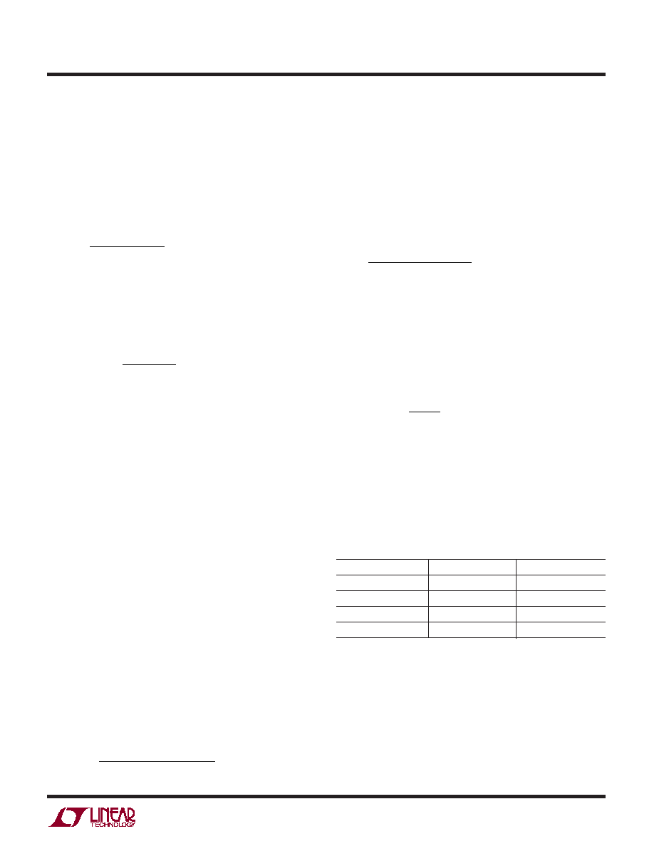
The minimum input voltage required to generate a particu-
lar output voltage in an LT3470 application is limited by
either its 4V undervoltage lockout or by its maximum duty
cycle. The duty cycle is the fraction of time that the internal
switch is on and is determined by the input and output
voltages:
DC
VV
V
OUT
D
IN
SW
D
=
+
–
where VD is the forward voltage drop of the catch diode
(~0.6V) and VSW is the voltage drop of the internal switch
at maximum load (~0.4V). Given DCMAX = 0.90, this leads
to a minimum input voltage of:
V
VV
DC
VV
IN MIN
OUT
D
MAX
SW
D
()
–
=
+
+
This analysis assumes the part has started up such that the
capacitor tied between the BOOST and SW pins is charged
to more than 2V. For proper start-up, the minimum input
voltage is limited by the boost circuit as detailed in the
section BOOST Pin Considerations.
The maximum input voltage is limited by the absolute
maximum VIN rating of 40V, provided an inductor of
sufficient value is used.
Inductor Selection
The switching action of the LT3470 during continuous
operation produces a square wave at the SW pin that
results in a triangle wave of current in the inductor. The
hysteretic mode control regulates the top and bottom
current limits (see Electrical Characteristics) such that the
average inductor current equals the load current. For safe
operation, it must be noted that the LT3470 cannot turn the
switch on for less than ~150ns. If the inductor is small and
the input voltage is high, the current through the switch
may exceed safe operating limit before the LT3470 is able
to turn off. To prevent this from happening, the following
equation provides a minimum inductor value:
L
Vt
I
MIN
IN MAX
MAX
=
() ON-TIME(MIN)
where VIN(MAX) is the maximum input voltage for the
application, tON-TIME(MIN) is ~150ns and IMAX is the maxi-
mum allowable increase in switch current during a mini-
mum switch on-time (150mA). While this equation provides
a safe inductor value, the resulting application circuit may
switch at too high a frequency to yield good efficiency. It
is advised that switching frequency be below 1.2MHz
during normal operation:
f
DC V
V
LI
D
OUT
L
= ()
+
()
1–
where f is the switching frequency,
IListheripplecurrent
in the inductor (~150mA), VD is the forward voltage drop
of the catch diode, and VOUT is the desired output voltage.
If the application circuit is intended to operate at high duty
cycles (VIN close to VOUT), it is important to look at the
calculated value of the switch off-time:
t
DC
f
OFF-TIME =
1–
The calculated tOFF-TIME should be more than LT3470’s
minimum tOFF-TIME (See Electrical Characteristics), so the
application circuit is capable of delivering full rated output
current. If the full output current of 200mA is not required,
the calculated tOFF-TIME can be made less than minimum
tOFF-TIME possibly allowing the use of a smaller inductor.
See Table 1 for an inductor value selection guide.
Table 1. Recommended Inductors for Loads up to 200mA
VOUT
VIN Up to 16V
VIN Up to 40V
2.5V
10
H33H
3.3V
10
H33H
5V
15
H33H
12V
33
H47H
Choose an inductor that is intended for power applica-
tions. Table 2 lists several manufacturers and inductor
series.
For robust output short-circuit protection at high VIN (up
to 40V) use at least a 33
H inductor with a minimum
450mA saturation current. If short-circuit performance is
not required, inductors with ISAT of 300mA or more may
相关PDF资料 |
PDF描述 |
|---|---|
| LT3470ITS8#PBF | 0.2 A SWITCHING REGULATOR, PDSO8 |
| LT3470HTS8#TR | SWITCHING REGULATOR, PDSO8 |
| LT3495BEDDB#PBF | 0.78 A SWITCHING REGULATOR, PDSO10 |
| LT3495BEDDB-1#PBF | 0.45 A SWITCHING REGULATOR, PDSO10 |
| LT3495EDDB-1#PBF | 0.45 A SWITCHING REGULATOR, PDSO10 |
相关代理商/技术参数 |
参数描述 |
|---|---|
| LT3470HDDB#TRMPBF | 功能描述:IC REG BUCK ADJ 0.2A 8DFN RoHS:是 类别:集成电路 (IC) >> PMIC - 稳压器 - DC DC 开关稳压器 系列:- 标准包装:2,500 系列:- 类型:降压(降压) 输出类型:固定 输出数:1 输出电压:1.2V,1.5V,1.8V,2.5V 输入电压:2.7 V ~ 20 V PWM 型:- 频率 - 开关:- 电流 - 输出:50mA 同步整流器:是 工作温度:-40°C ~ 125°C 安装类型:表面贴装 封装/外壳:10-TFSOP,10-MSOP(0.118",3.00mm 宽)裸露焊盘 包装:带卷 (TR) 供应商设备封装:10-MSOP 裸露焊盘 |
| LT3470HDDB#TRPBF | 功能描述:IC REG BUCK ADJ 0.2A 8DFN RoHS:是 类别:集成电路 (IC) >> PMIC - 稳压器 - DC DC 开关稳压器 系列:- 标准包装:2,500 系列:- 类型:降压(降压) 输出类型:固定 输出数:1 输出电压:1.2V,1.5V,1.8V,2.5V 输入电压:2.7 V ~ 20 V PWM 型:- 频率 - 开关:- 电流 - 输出:50mA 同步整流器:是 工作温度:-40°C ~ 125°C 安装类型:表面贴装 封装/外壳:10-TFSOP,10-MSOP(0.118",3.00mm 宽)裸露焊盘 包装:带卷 (TR) 供应商设备封装:10-MSOP 裸露焊盘 |
| LT3470HTS8 | 制造商:LINER 制造商全称:Linear Technology 功能描述:Micropower Buck Regulator with Integrated Boost and Catch Diodes |
| LT3470HTS8#PBF | 制造商:Linear Technology 功能描述:SP-SWREG/Monolithic, Cut Tape 300mA, 40V MicroPower Step-Down Regulator with Int |
| LT3470HTS8#TRMPBF | 功能描述:IC REG BUCK ADJ 0.2A TSOT23-8 RoHS:是 类别:集成电路 (IC) >> PMIC - 稳压器 - DC DC 开关稳压器 系列:- 标准包装:2,500 系列:- 类型:降压(降压) 输出类型:固定 输出数:1 输出电压:1.2V,1.5V,1.8V,2.5V 输入电压:2.7 V ~ 20 V PWM 型:- 频率 - 开关:- 电流 - 输出:50mA 同步整流器:是 工作温度:-40°C ~ 125°C 安装类型:表面贴装 封装/外壳:10-TFSOP,10-MSOP(0.118",3.00mm 宽)裸露焊盘 包装:带卷 (TR) 供应商设备封装:10-MSOP 裸露焊盘 |
发布紧急采购,3分钟左右您将得到回复。