- 您现在的位置:买卖IC网 > PDF目录13956 > LT3480EDD#TRPBF (Linear Technology)IC REG BUCK ADJ 2A 10DFN PDF资料下载
参数资料
| 型号: | LT3480EDD#TRPBF |
| 厂商: | Linear Technology |
| 文件页数: | 7/24页 |
| 文件大小: | 0K |
| 描述: | IC REG BUCK ADJ 2A 10DFN |
| 标准包装: | 2,500 |
| 类型: | 降压(降压) |
| 输出类型: | 可调式 |
| 输出数: | 1 |
| 输出电压: | 0.79 V ~ 20 V |
| 输入电压: | 3.6 V ~ 36 V |
| PWM 型: | 电流模式,混合 |
| 频率 - 开关: | 200kHz ~ 2.4MHz |
| 电流 - 输出: | 2A |
| 同步整流器: | 无 |
| 工作温度: | -40°C ~ 85°C |
| 安装类型: | 表面贴装 |
| 封装/外壳: | 10-WFDFN 裸露焊盘 |
| 包装: | 带卷 (TR) |
| 供应商设备封装: | 10-DFN(3x3) |
�� �
�
�LT3480�
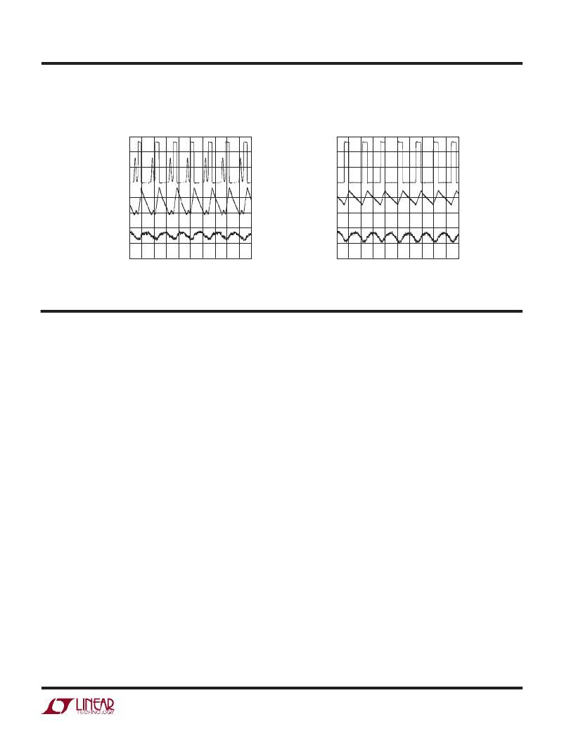
�TYPICAL� PERFORMANCE� CHARACTERISTICS�
�V� SW�
�5V/DIV�
�I� L�
�0.2A/DIV�
�V� OUT�
�10mV/DIV�
�Switching� Waveforms;� Transition�
�from� Burst� Mode� to� Full� Frequency�
�V� SW�
�5V/DIV�
�I� L�
�0.5A/DIV�
�V� OUT�
�10mV/DIV�
�Switching� Waveforms;� Full�
�Frequency� Continuous� Operation�
�1μs/DIV�
�V� IN� =� 12V;� FRONT� PAGE� APPLICATION�
�I� LOAD� =� 110mA�
�3480� G25�
�1μs/DIV�
�V� IN� =� 12V;� FRONT� PAGE� APPLICATION�
�I� LOAD� =� 1A�
�3480� G26�
�PIN� FUNCTIONS�
�BD� (Pin� 1):� This� pin� connects� to� the� anode� of� the� boost�
�Schottky� diode.� BD� also� supplies� current� to� the� internal�
�regulator.� BD� must� be� locally� bypassed� when� not� tied� to�
�V� OUT� with� a� low� ESR� capacitor� (1μF).�
�BOOST� (Pin� 2):� This� pin� is� used� to� provide� a� drive�
�voltage,� higher� than� the� input� voltage,� to� the� internal� bipolar�
�NPN� power� switch.�
�SW� (Pin� 3):� The� SW� pin� is� the� output� of� the� internal� power�
�switch.� Connect� this� pin� to� the� inductor,� catch� diode� and�
�boost� capacitor.�
�V� IN� (Pin� 4):� The� V� IN� pin� supplies� current� to� the� LT3480’s�
�internal� regulator� and� to� the� internal� power� switch.� This�
�pin� must� be� locally� bypassed.�
�RUN/SS� (Pin� 5):� The� RUN/SS� pin� is� used� to� put� the�
�LT3480� in� shutdown� mode.� Tie� to� ground� to� shut� down�
�the� LT3480.� Tie� to� 2.5V� or� more� for� normal� operation.� If�
�the� shutdown� feature� is� not� used,� tie� this� pin� to� the� V� IN�
�pin.� RUN/SS� also� provides� a� soft-start� function;� see� the�
�Applications� Information� section.�
�SYNC� (Pin� 6):� This� is� the� external� clock� synchronization�
�input.� Ground� this� pin� for� low� ripple� Burst� Mode� operation� at�
�low� output� loads.� Tie� to� a� clock� source� for� synchronization.�
�Clock� edges� should� have� rise� and� fall� times� faster� than� 1μs.�
�See� synchronizing� section� in� Applications� Information.�
�PG� (Pin� 7):� The� PG� pin� is� the� open� collector� output� of� an�
�internal� comparator.� PG� remains� low� until� the� FB� pin� is�
�within� 14%� of� the� final� regulation� voltage.� PG� output� is�
�valid� when� V� IN� is� above� 3.6V� and� RUN/SS� is� high.�
�FB� (Pin� 8):� The� LT3480� regulates� the� FB� pin� to� 0.790V.�
�Connect� the� feedback� resistor� divider� tap� to� this� pin.�
�V� C� (Pin� 9):� The� V� C� pin� is� the� output� of� the� internal� error�
�amplifier.� The� voltage� on� this� pin� controls� the� peak� switch�
�current.� Tie� an� RC� network� from� this� pin� to� ground� to�
�compensate� the� control� loop.�
�RT� (Pin� 10):� Oscillator� Resistor� Input.� Connecting� a� resistor�
�to� ground� from� this� pin� sets� the� switching� frequency.�
�Exposed� Pad� (Pin� 11):� Ground.� The� exposed� pad� must�
�be� soldered� to� PCB.�
�3480fe�
�For� more� information� www.linear.com/LT3480�
�7�
�相关PDF资料 |
PDF描述 |
|---|---|
| HM73-106R0LFTR13 | INDUCTOR 6.0UH LOW PRO SHLD SMD |
| ESM28DRXH | CONN EDGECARD 56POS DIP .156 SLD |
| HM73-151R5LFTR13 | INDUCTOR 1.5UH LOW PRO SHLD SMD |
| ECM43DRTI | CONN EDGECARD 86POS DIP .156 SLD |
| HM55-21R95LF | SHIELDED DRUM COMPACT INDUCTOR |
相关代理商/技术参数 |
参数描述 |
|---|---|
| LT3480EMSE | 制造商:LINER 制造商全称:Linear Technology 功能描述:36V, 2A, 2.4MHz Step-Down Switching Regulator with 70μA Quiescent Current |
| LT3480EMSE#PBF | 功能描述:IC REG BUCK ADJ 2A 10MSOP RoHS:是 类别:集成电路 (IC) >> PMIC - 稳压器 - DC DC 开关稳压器 系列:- 标准包装:250 系列:- 类型:降压(降压) 输出类型:固定 输出数:1 输出电压:1.2V 输入电压:2.05 V ~ 6 V PWM 型:电压模式 频率 - 开关:2MHz 电流 - 输出:500mA 同步整流器:是 工作温度:-40°C ~ 85°C 安装类型:表面贴装 封装/外壳:6-UFDFN 包装:带卷 (TR) 供应商设备封装:6-SON(1.45x1) 产品目录页面:1032 (CN2011-ZH PDF) 其它名称:296-25628-2 |
| LT3480EMSE#PBF | 制造商:Linear Technology 功能描述:DC/DC Converter IC 制造商:Linear Technology 功能描述:IC, BUCK REGULATOR, MSOP-10 |
| LT3480EMSE#TRPBF | 功能描述:IC REG BUCK ADJ 2A 10MSOP RoHS:是 类别:集成电路 (IC) >> PMIC - 稳压器 - DC DC 开关稳压器 系列:- 标准包装:2,500 系列:- 类型:降压(降压) 输出类型:固定 输出数:1 输出电压:1.2V,1.5V,1.8V,2.5V 输入电压:2.7 V ~ 20 V PWM 型:- 频率 - 开关:- 电流 - 输出:50mA 同步整流器:是 工作温度:-40°C ~ 125°C 安装类型:表面贴装 封装/外壳:10-TFSOP,10-MSOP(0.118",3.00mm 宽)裸露焊盘 包装:带卷 (TR) 供应商设备封装:10-MSOP 裸露焊盘 |
| LT3480EMSEPBF | 制造商:Linear Technology 功能描述:Conv DC-DC Single-Out Step Down |
发布紧急采购,3分钟左右您将得到回复。