参数资料
| 型号: | LT3493IDCB#TRMPBF |
| 厂商: | Linear Technology |
| 文件页数: | 8/20页 |
| 文件大小: | 0K |
| 描述: | IC REG BUCK ADJ 1.2A 6DFN |
| 标准包装: | 500 |
| 类型: | 降压(降压) |
| 输出类型: | 可调式 |
| 输出数: | 1 |
| 输出电压: | 0.78 V ~ 34.2 V |
| 输入电压: | 3.6 V ~ 36 V |
| PWM 型: | 电流模式 |
| 频率 - 开关: | 750kHz |
| 电流 - 输出: | 1.2A |
| 同步整流器: | 无 |
| 工作温度: | -40°C ~ 125°C |
| 安装类型: | 表面贴装 |
| 封装/外壳: | 6-WFDFN 裸露焊盘 |
| 包装: | 带卷 (TR) |
| 供应商设备封装: | 6-DFN-EP(2x3) |
�� �
�
�LT3493�
�APPLICATIONS� INFORMATION�
�FB� Resistor� Network�
�The� output� voltage� is� programmed� with� a� resistor� divider�
�between� the� output� and� the� FB� pin.� Choose� the� 1%� resis-�
�tors� according� to:�
�of� the� V� IN� and� BOOST� pins.� The� input� voltage� should� be�
�limited� to� the� V� IN� operating� range� (36V)� during� overload�
�conditions� (short-circuit� or� start-up).�
�Minimum� On� Time�
�R1� =� R2�
�V� OUT�
�0.78V�
�–1�
�The� part� will� still� regulate� the� output� at� input� voltages� that�
�exceed� V� IN(MAX)� (up� to� 40V),� however,� the� output� voltage�
�R2� should� be� 20k� or� less� to� avoid� bias� current� errors.�
�Reference� designators� refer� to� the� Block� Diagram.�
�An� optional� phase� lead� capacitor� of� 22pF� between� V� OUT�
�and� FB� reduces� light-load� output� ripple.�
�Input� Voltage� Range�
�The� input� voltage� range� for� LT3493� applications� depends�
�on� the� output� voltage� and� on� the� absolute� maximum� rat-�
�ings� of� the� V� IN� and� BOOST� pins.�
�The� minimum� input� voltage� is� determined� by� either� the�
�LT3493’s� minimum� operating� voltage� of� 3.6V,� or� by� its�
�maximum� duty� cycle.� The� duty� cycle� is� the� fraction� of�
�time� that� the� internal� switch� is� on� and� is� determined� by�
�the� input� and� output� voltages:�
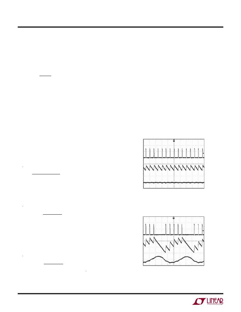
�ripple� increases� as� the� input� voltage� is� increased.� Figure� 1�
�illustrates� switching� waveforms� in� continuous� mode� for� a�
�3V� output� application� near� V� IN(MAX)� =� 33V.�
�As� the� input� voltage� is� increased,� the� part� is� required�
�to� switch� for� shorter� periods� of� time.� Delays� associated�
�with� turning� off� the� power� switch� dictate� the� minimum�
�on� time� of� the� part.� The� minimum� on� time� for� the� LT3493�
�is� ~120ns.� Figure� 2� illustrates� the� switching� waveforms�
�when� the� input� voltage� is� increased� to� V� IN� =� 35V.�
�V� SW�
�20V/DIV�
�DC� =�
�V� OUT� +� V� D�
�V� IN� –� V� SW� +� V� D�
�I� L�
�0.5A/DIV�
�V� OUT�
�where� V� D� is� the� forward� voltage� drop� of� the� catch� diode�
�200mV/DIV�
�AC� COUPLED�
�(~0.4V)� and� V� SW� is� the� voltage� drop� of� the� internal� switch�
�(~0.4V� at� maximum� load).� This� leads� to� a� minimum� input�
�voltage� of:�
�C� OUT� =� 10μF�
�V� OUT� =� 3V�
�V� IN� =� 30V�
�I� LOAD� =� 0.75A�
�L� =� 10μH�
�2μs/DIV�
�3493� F01�
�V� IN(MIN)� =�
�V� OUT� +� V� D�
�DC� MAX�
�–� V� D� +� V� SW�
�Figure� 1�
�with� DC� MAX� =� 0.91� (0.88� over� temperature).�
�The� maximum� input� voltage� is� determined� by� the� absolute�
�maximum� ratings� of� the� V� IN� and� BOOST� pins.� For� con-�
�tinuous� mode� operation,� the� maximum� input� voltage� is�
�determined� by� the� minimum� duty� cycle� DC� MIN� =� 0.10:�
�V� SW�
�20V/DIV�
�I� L�
�0.5A/DIV�
�V� OUT� +� V� D�
�DC� MIN�
�V� IN(MAX)� = – V� D� +V� SW�
�Note� that� this� is� a� restriction� on� the� operating� input� voltage�
�for� continuous� mode� operation;� the� circuit� will� tolerate�
�V� OUT�
�200mV/DIV�
�AC� COUPLED�
�C� OUT� =� 10μF�
�V� OUT� =� 3V�
�V� IN� =� 35V�
�I� LOAD� =� 0.75A�
�L� =� 10μH�
�2μs/DIV�
�3493� F02�
�transient� inputs� up� to� the� absolute� maximum� ratings�
�Figure� 2�
�3493fb�
�8�
�相关PDF资料 |
PDF描述 |
|---|---|
| LT3494EDDB#TRPBF | IC REG BOOST ADJ 0.18A 8DFN |
| LT3495EDDB-1#TRMPBF | IC REG BOOST ADJ 0.35A 10DFN |
| LT3501IFE#TRPBF | IC REG BUCK ADJ 3A DL 20TSSOP |
| LT3502IMS#TRPBF | IC REG BUCK ADJ 0.5A 10MSOP |
| LT3503EDCB#TRPBF | IC REG BUCK ADJ 1A 6DFN |
相关代理商/技术参数 |
参数描述 |
|---|---|
| LT3493IDCB-TRPBF | 制造商:LINER 制造商全称:Linear Technology 功能描述:1.2A, 750kHz Step-Down Switching Regulator in 2mm × 3mm DFN |
| LT3494 | 制造商:LINER 制造商全称:Linear Technology 功能描述:Micropower Low Noise Boost Converters with Output Disconnect |
| LT3494A | 制造商:LINER 制造商全称:Linear Technology 功能描述:20mA LED Driver and OLED Driver with Integrated Schottky in 3mm x 2mm DFN |
| LT3494AEDDB | 制造商:LINER 制造商全称:Linear Technology 功能描述:Micropower Low Noise Boost Converters with Output Disconnect |
| LT3494AEDDB#PBF | 制造商:Linear Technology 功能描述:BOOST 2.3 - 16V 0.35A 40V 制造商:Linear Technology 功能描述:BOOST, 2.3 - 16V, 0.35A, 40V, 20QFN |
发布紧急采购,3分钟左右您将得到回复。