- 您现在的位置:买卖IC网 > PDF目录20625 > LT3500HDD#PBF (Linear Technology)IC REG DL BUCK/LINEAR 12-DFN PDF资料下载
参数资料
| 型号: | LT3500HDD#PBF |
| 厂商: | Linear Technology |
| 文件页数: | 12/28页 |
| 文件大小: | 322K |
| 描述: | IC REG DL BUCK/LINEAR 12-DFN |
| 标准包装: | 121 |
| 拓扑: | 降压(降压)(1),线性(LDO)(1) |
| 功能: | 任何功能 |
| 输出数: | 2 |
| 频率 - 开关: | 500kHz ~ 2.4MHz |
| 电压/电流 - 输出 1: | 0.8 V ~ 38.9 V,2A |
| 电压/电流 - 输出 2: | 可调式,13mA |
| 带 LED 驱动器: | 无 |
| 带监控器: | 无 |
| 带序列发生器: | 无 |
| 电源电压: | 3 V ~ 36 V |
| 工作温度: | -40°C ~ 150°C |
| 安装类型: | 表面贴装 |
| 封装/外壳: | 12-WFDFN 裸露焊盘 |
| 供应商设备封装: | 12-DFN |
| 包装: | 管件 |
| 产品目录页面: | 1331 (CN2011-ZH PDF) |
第1页第2页第3页第4页第5页第6页第7页第8页第9页第10页第11页当前第12页第13页第14页第15页第16页第17页第18页第19页第20页第21页第22页第23页第24页第25页第26页第27页第28页
LT3500
12
3500fc
APPLICATIONS INFORMATION
Table 1. Ef ciency and Size Comparisons for Different R
RT/SYNC
Values, V
OUT1
= 3.3V
FREQUENCY
R
T
/SYNC
EFFICIENCY
V
IN(MAX)
L
C
C + L AREA
(mm
2
)
2.5MHz
15k
73.6
12
1?/DIV>
10?/DIV>
24
2.0MHz
20k
81.5
14
1.5?/DIV>
10?/DIV>
24
1.5MHz
24.9k
84.5
18
2.2?/DIV>
10?/DIV>
24
1.0MHz
40.2k
87.3
28
3.3?/DIV>
22?/DIV>
34
500kHz
90.9k
88.9
36
4.7?/DIV>
47?/DIV>
40
The following example along with the data in Table 1
illustrates the tradeoffs of switch frequency selection.
Example.
V
IN
= 25V, V
OUT1
= 3.3V, I
OUT1
= 2.0A,
Temperature = 0癈 to 85癈
t
ON(MIN)
= 185ns (85癈 from Typical Characteris-
tics graph), V
D
= 0.6V, V
SW
= 0.4V (85癈)
Max Frequency=
3.3+0.6
250.4+0.6
"
1
185ns
~835kHz
R
T
/SYNC ~ 49.9k
Frequency E 820kHz
Input Voltage Range
Once the switching frequency has been determined, the
input voltage range of the regulator can be determined.
The minimum input voltage is determined by either the
LT3500s minimum operating voltage of ~2.8V or by its
maximum duty cycle. The duty cycle is the fraction of time
that the internal switch is on during a clock cycle. The
maximum duty cycle can be determined from the clock
frequency and the minimum off time from the typical
characteristics graph.
This leads to a minimum input voltage of:
V
IN(MIN)
=
V
OUT1
+V
D
DC
MAX
V
D
+V
SW
where V
SW
is the voltage drop of the internal switch,
and
DC
MAX
= 1 t
OFF(MIN)
" Frequency.
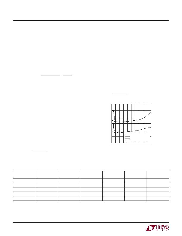
Figure 3 shows a typical graph of minimum input voltage
vs load current for 3.3V and 5V applications.
The maximum input voltage is determined by the absolute
maximum ratings of the V
IN
and BST pins and by the
frequency and minimum duty cycle.
The minimum duty cycle is de ned as:
DC
MIN
= t
ON(MIN)
" Frequency
Maximum input voltage as:
V
IN(MAX)
=
V
OUT1
+V
D
DC
MIN
V
D
+V
SW
Figure 3. Minimum Input Voltage vs Load Current
LOAD CURRENT (A)
0
3
4
5
1.0
1.6 1.8
3500 F03
2
0.2 0.4 0.6 0.8
1.4
1.2
6
7
8
2.0
V
OUT1
= 5V START-UP
V
OUT1
= 5V RUNNING
V
OUT1
= 3.3V START-UP
V
OUT1
= 3.3V RUNNING
f
SW
= 1MHz
L = 3.3糎
相关PDF资料 |
PDF描述 |
|---|---|
| LT3500IMSE#PBF | IC REG DL BUCK/LINEAR 16-MSOP |
| LTC1704BEGN | IC REG DL BUCK/LINEAR 16-SSOP |
| GBM22DRXN | CONN EDGECARD 44POS DIP .156 SLD |
| ADE7759ARSZRL | IC ENERGY METERING 1PHASE 20SSOP |
| LTC1704BEGN#PBF | IC REG DL BUCK/LINEAR 16-SSOP |
相关代理商/技术参数 |
参数描述 |
|---|---|
| LT3500HDD-TRPBF | 制造商:LINER 制造商全称:Linear Technology 功能描述:Monolithic 2A Step-Down Regulator Plus Linear Regulator/Controller |
| LT3500HMSE#PBF | 功能描述:IC REG DL BUCK/LINEAR 16-MSOP RoHS:是 类别:集成电路 (IC) >> PMIC - 稳压器 - 线性 + 切换式 系列:- 标准包装:2,500 系列:- 拓扑:降压(降压)同步(3),线性(LDO)(2) 功能:任何功能 输出数:5 频率 - 开关:300kHz 电压/电流 - 输出 1:控制器 电压/电流 - 输出 2:控制器 电压/电流 - 输出 3:控制器 带 LED 驱动器:无 带监控器:无 带序列发生器:是 电源电压:5.6 V ~ 24 V 工作温度:-40°C ~ 85°C 安装类型:* 封装/外壳:* 供应商设备封装:* 包装:* |
| LT3500HMSE#TRPBF | 功能描述:IC REG DL BUCK/LINEAR 16-MSOP RoHS:是 类别:集成电路 (IC) >> PMIC - 稳压器 - 线性 + 切换式 系列:- 标准包装:2,500 系列:- 拓扑:降压(降压)同步(3),线性(LDO)(2) 功能:任何功能 输出数:5 频率 - 开关:300kHz 电压/电流 - 输出 1:控制器 电压/电流 - 输出 2:控制器 电压/电流 - 输出 3:控制器 带 LED 驱动器:无 带监控器:无 带序列发生器:是 电源电压:5.6 V ~ 24 V 工作温度:-40°C ~ 85°C 安装类型:* 封装/外壳:* 供应商设备封装:* 包装:* |
| LT3500HMSE-PBF | 制造商:LINER 制造商全称:Linear Technology 功能描述:Monolithic 2A Step-Down Regulator Plus Linear Regulator/Controller |
| LT3500HMSE-TRPBF | 制造商:LINER 制造商全称:Linear Technology 功能描述:Monolithic 2A Step-Down Regulator Plus Linear Regulator/Controller |
发布紧急采购,3分钟左右您将得到回复。