- 您现在的位置:买卖IC网 > PDF目录20625 > LT3500HDD#PBF (Linear Technology)IC REG DL BUCK/LINEAR 12-DFN PDF资料下载
参数资料
| 型号: | LT3500HDD#PBF |
| 厂商: | Linear Technology |
| 文件页数: | 17/28页 |
| 文件大小: | 322K |
| 描述: | IC REG DL BUCK/LINEAR 12-DFN |
| 标准包装: | 121 |
| 拓扑: | 降压(降压)(1),线性(LDO)(1) |
| 功能: | 任何功能 |
| 输出数: | 2 |
| 频率 - 开关: | 500kHz ~ 2.4MHz |
| 电压/电流 - 输出 1: | 0.8 V ~ 38.9 V,2A |
| 电压/电流 - 输出 2: | 可调式,13mA |
| 带 LED 驱动器: | 无 |
| 带监控器: | 无 |
| 带序列发生器: | 无 |
| 电源电压: | 3 V ~ 36 V |
| 工作温度: | -40°C ~ 150°C |
| 安装类型: | 表面贴装 |
| 封装/外壳: | 12-WFDFN 裸露焊盘 |
| 供应商设备封装: | 12-DFN |
| 包装: | 管件 |
| 产品目录页面: | 1331 (CN2011-ZH PDF) |
第1页第2页第3页第4页第5页第6页第7页第8页第9页第10页第11页第12页第13页第14页第15页第16页当前第17页第18页第19页第20页第21页第22页第23页第24页第25页第26页第27页第28页
LT3500
17
3500fc
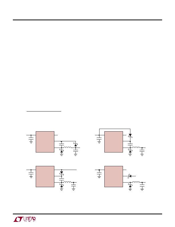
Figure 5. BST Pin Considerations
V
BST
V
SW
= V
X
V
BST(MAX)
= V
X
V
X
> V
IN
+ 3V
(5d)
(5c)
(5b)
V
BST
V
SW
= V
IN
V
BST(MAX)
= 2 "燰
IN
V
IN
V
IN
D2
D1
D1
D1
D1
(5a)
LT3500
LDRV
BST
SW
V
BST
V
SW
= V
OUT1
V
BST(MAX)
= V
IN
+ V
OUT1
V
BST
V
SW
= V
OUT2
V
BST(MAX)
= V
IN
+ V
OUT2
V
OUT2
e 2.5V
V
OUT1
V
OUT2
C3
V
IN
V
IN
D2
LT3500
LDRV
BST
SW
V
OUT1
V
IN
V
IN
LT3500
LDRV
BST
SW
V
OUT1
C3
V
IN
V
IN
D2
LT3500
LDRV
BST
SW
D2
V
OUT1
C3
3500 F05
The only reason to consider a larger diode is the worst-
case condition of a high input voltage and shorted output.
With a shorted condition, diode current will increase to a
typical value of 3A, determined by the peak switch current
limit of the LT3500. This is safe for short periods of time,
but it would be prudent to check with the diode manu-
facturer if continuous operation under these conditions
can be tolerated.
BST Pin Considerations
The capacitor and diode tied to the BST pin generate
a voltage that is higher than the input voltage. In most
cases a 0.47糉 capacitor and fast switching diode (such
as the CMDSH-3 or FMMD914) will work well. Almost
any type of lm or ceramic capacitor is suitable, but the
ESR should be <1?to ensure it can be fully recharged
during the off time of the switch. The capacitor value can
be approximated by:
C
BST
=
I
OUT1(MAX)
"DC
50" V
OUT1
V
BST(MIN)
(
)
"f
where I
OUT1(MAX)
is the maximum load current, and
V
BST(MIN)
is the minimum boost voltage to fully saturate
the switch.
Figure 5 shows four ways to arrange the boost circuit.
The BST pin must be more than 2.2V above the SW pin
for full ef ciency.
Generally, for outputs of 3.3V and higher the standard
circuit (Figure 5a) is the best. For outputs between 2.8V
and 3.3V, replace the D2 with a small Schottky diode such
as the PMEG4005.
For lower output voltages the boost diode can be tied to
the input (Figure 5b). The circuit in Figure 5a is more ef-
cient because the BST pin current comes from a lower
voltage source.
Figure 5c shows the boost voltage source from the linear
output that is set to greater than 2.5V (any available DC
sources that are greater than 2.5V is suf cient). The highest
ef ciency is attained by choosing the lowest boost volt-
age above 2.5V. You must also be sure that the maximum
voltage at the BST pin is less than the maximum speci ed
in the Absolute Maximum Ratings section.
APPLICATIONS INFORMATION
相关PDF资料 |
PDF描述 |
|---|---|
| LT3500IMSE#PBF | IC REG DL BUCK/LINEAR 16-MSOP |
| LTC1704BEGN | IC REG DL BUCK/LINEAR 16-SSOP |
| GBM22DRXN | CONN EDGECARD 44POS DIP .156 SLD |
| ADE7759ARSZRL | IC ENERGY METERING 1PHASE 20SSOP |
| LTC1704BEGN#PBF | IC REG DL BUCK/LINEAR 16-SSOP |
相关代理商/技术参数 |
参数描述 |
|---|---|
| LT3500HDD-TRPBF | 制造商:LINER 制造商全称:Linear Technology 功能描述:Monolithic 2A Step-Down Regulator Plus Linear Regulator/Controller |
| LT3500HMSE#PBF | 功能描述:IC REG DL BUCK/LINEAR 16-MSOP RoHS:是 类别:集成电路 (IC) >> PMIC - 稳压器 - 线性 + 切换式 系列:- 标准包装:2,500 系列:- 拓扑:降压(降压)同步(3),线性(LDO)(2) 功能:任何功能 输出数:5 频率 - 开关:300kHz 电压/电流 - 输出 1:控制器 电压/电流 - 输出 2:控制器 电压/电流 - 输出 3:控制器 带 LED 驱动器:无 带监控器:无 带序列发生器:是 电源电压:5.6 V ~ 24 V 工作温度:-40°C ~ 85°C 安装类型:* 封装/外壳:* 供应商设备封装:* 包装:* |
| LT3500HMSE#TRPBF | 功能描述:IC REG DL BUCK/LINEAR 16-MSOP RoHS:是 类别:集成电路 (IC) >> PMIC - 稳压器 - 线性 + 切换式 系列:- 标准包装:2,500 系列:- 拓扑:降压(降压)同步(3),线性(LDO)(2) 功能:任何功能 输出数:5 频率 - 开关:300kHz 电压/电流 - 输出 1:控制器 电压/电流 - 输出 2:控制器 电压/电流 - 输出 3:控制器 带 LED 驱动器:无 带监控器:无 带序列发生器:是 电源电压:5.6 V ~ 24 V 工作温度:-40°C ~ 85°C 安装类型:* 封装/外壳:* 供应商设备封装:* 包装:* |
| LT3500HMSE-PBF | 制造商:LINER 制造商全称:Linear Technology 功能描述:Monolithic 2A Step-Down Regulator Plus Linear Regulator/Controller |
| LT3500HMSE-TRPBF | 制造商:LINER 制造商全称:Linear Technology 功能描述:Monolithic 2A Step-Down Regulator Plus Linear Regulator/Controller |
发布紧急采购,3分钟左右您将得到回复。